Terafab Meaning and Concept Explained: A 2026 Guide
Terafab sounds like a factory story. It's really a control story.
Public reporting describes Terafab as a named semiconductor project announced on March 21, 2026 in Austin, Texas, with a reported initial investment of roughly $20 billion to $25 billion and a long-run goal of 1 terawatt of AI compute per year, according to MarketWise's report on the Terafab chip factory. That framing matters because Terafab isn't being pitched as one more fab in an already crowded industrial category. It's being pitched as a way to pull design, fabrication, packaging, and testing into one production base for Tesla, SpaceX, and xAI.
That's why the phrase Terafab meaning and concept explained needs more than a simple definition. The core question isn't just what Terafab means. It's whether this kind of industrial system can be built at the scale implied by the public narrative.
Table of Contents
- Introduction
- Deconstructing the Terafab Vision
- Understanding Vertical Integration in Chipmaking
- How a Terafab Aims to Operate
- Target Applications and Use Cases
- Feasibility Hurdles and Investment Risks
- Broader Implications for the AI and Tech Industries
- Frequently Asked Questions About Terafab
Introduction
Terafab is a specific project name, not a generic industry term. In current public reporting, it refers to a planned vertically integrated semiconductor facility in Austin, Texas, tied to Elon Musk's industrial ecosystem and described as combining chip functions that most companies spread across multiple suppliers.
That distinction matters because people searching for Terafab meaning usually expect a vocabulary answer. What they need is an industrial one. The name points to a vision in which one facility handles more of the semiconductor stack than the modern industry typically allows.
The attraction is easy to see. If one organization can design its own chips, manufacture them, package them, and test them in a tightly connected loop, it may reduce delays, reduce handoffs, and align chip development more closely with end products like autonomous systems, robots, and AI infrastructure.
Practical rule: When a project claims to compress the whole chip pipeline into one system, the first question isn't “Is this bold?” It's “Which bottlenecks is it trying to remove, and what new bottlenecks does it create?”
The harder part is feasibility. Terafab's meaning only becomes clear when you hold the vision next to the realities of fab economics, specialized labor, equipment supply, and the difference between a captive internal manufacturing base and a true merchant foundry.
Deconstructing the Terafab Vision

A proper noun with industrial ambition
Terafab refers to a specific semiconductor project centered in Austin, Texas, publicly described with a multibillion-dollar investment range, a 2026 launch announcement, and an unusually large compute target. Those details matter because they place the term in the category of industrial strategy, not general manufacturing jargon.
That framing changes how the project should be evaluated.
A named facility with a defined location, timeline, and captive customer base invites a different question from the one many explainers ask. The central question is less "what does the word mean?" and more "can this operating model be built at the scale being implied?" In semiconductors, ambition is common. Execution at this level is rare, expensive, and constrained by equipment availability, process know-how, and years of yield learning.
Public descriptions also connect Terafab to demand from Tesla, SpaceX, and xAI. That suggests a supply strategy designed around internal consumption rather than a broad merchant foundry model. The distinction is economically important. A captive fab can justify investments that would look questionable for an open-market supplier, but it also depends on those affiliated companies generating stable, high-volume demand over a long period.
Why the concept stands out
The usual chip supply chain works like a relay. Design, wafer fabrication, packaging, and testing often sit with different specialists, each optimized for its own part of the process. Terafab proposes to compress more of that chain into one coordinated system.
| Model | How it works | Main strength | Main weakness |
|---|---|---|---|
| Fragmented chip model | Separate firms handle design, fabrication, packaging, and testing | Deep specialization | More handoffs and coordination risk |
| Terafab concept | One integrated system handles more of the pipeline internally | Faster feedback and tighter control | Much harder to build and manage |
The attraction is obvious. Fewer organizational boundaries can shorten design cycles, reduce scheduling conflicts, and align manufacturing choices with product needs. For AI accelerators, automotive compute, or robotics hardware, that tighter loop could matter as much as raw wafer output.
But the harder analysis starts after that.
Vertical integration does not remove complexity. It changes who has to carry it. Under the Terafab model, one organization has to secure advanced tools, recruit process engineers, manage packaging capacity, maintain test infrastructure, and absorb the financial risk when one part of the chain slips. What looks efficient on a slide can become a concentration of operational risk on the factory floor.
The core claim behind Terafab is not just bigger chip production. It is tighter industrial coordination, with design, manufacturing, packaging, and validation feeding back into each other faster than the standard supplier network allows.
If that loop works, the payoff could be meaningful. If one link underperforms, the same integration that promises speed can magnify delays, because there are fewer external buffers to absorb mistakes. That feasibility gap is what makes Terafab interesting. The concept is easy to describe. Building it would require overcoming some of the semiconductor industry's most entrenched constraints.
Understanding Vertical Integration in Chipmaking

What gets pulled under one roof
Current public reporting describes Terafab as a planned vertically integrated semiconductor fabrication plant meant to consolidate chip design, fabrication, lithography, memory production, advanced packaging, and testing in one facility, with an initial prototype phase in Austin, according to the current Terafab overview on Wikipedia.
That list is what makes the concept unusual. Most chip programs move through a relay race of specialists. One team designs the architecture. Another organization manufactures the wafers. Another packages the dies. Another performs parts of qualification and testing. Every handoff introduces delay, interpretation risk, and commercial dependency.
Inside the Terafab concept, the wafer's journey is supposed to look more like a closed loop:
- Design begins in-house. Engineers define the chip around a known product need, not a generic merchant market.
- Fabrication happens inside the same system. Process teams and design teams can respond to each other more directly.
- Packaging stays integrated. Advanced packaging decisions can shape performance, thermals, and system fit.
- Testing closes the feedback loop. Manufacturing defects and performance issues feed back to design faster.
That's the strategic attraction of vertical integration. It shrinks the organizational distance between idea and finished silicon.
Why the chip industry usually stays fragmented
The current industry didn't become specialized by accident. It specialized because semiconductor manufacturing is punishingly expensive, operationally delicate, and dependent on narrow expertise.
A fabless company can focus on architecture and software. A foundry can focus on process technology and yield. Packaging houses can build deep competence around assembly techniques. Test specialists can optimize around reliability and validation.
Here's the tradeoff in simple terms:
| Question | Vertical integration | Fragmented specialization |
|---|---|---|
| Speed of iteration | Potentially faster | Often slower because of handoffs |
| Control over process | Higher if executed well | Shared across suppliers |
| Capital burden | Concentrated and heavy | Distributed across the ecosystem |
| Execution difficulty | Extremely high | Lower for any single participant |
The reason Terafab gets attention is that it challenges this established logic. It suggests that for AI systems, robotics, vehicles, and aerospace hardware, the old fragmentation may be too slow or too externally dependent.
That's why the model resonates with broader automation trends. If you've followed large-scale industrial automation, you can see parallels in how manufacturers try to compress feedback loops between design, production, and deployment, as discussed in this piece on China's industrial robot production surge and the new era in automation.
Analyst view: Vertical integration works best when the product roadmap is clear, internal demand is large, and the company can afford to optimize for long-term control instead of near-term financial neatness.
That last condition is the hardest one. A vertically integrated fab doesn't just need ambition. It needs staying power.
How a Terafab Aims to Operate

A captive system, not a foundry for everyone
One of the most important distinctions in any Terafab meaning and concept explained article is this one: neutral coverage describes Terafab less as a conventional merchant foundry and more as a form of vertical integration for Tesla, SpaceX, and xAI, according to Data Center Knowledge's analysis of Terafab and AI infrastructure.
That changes the operating logic.
A merchant foundry sells manufacturing capacity broadly. It serves many customers, absorbs many design styles, and lives or dies by neutrality, scale, cost, and yield. A captive fab system has a narrower mission. It exists to support internal demand and align silicon decisions with product strategy.
That means the operational workflow would likely prioritize product-specific chip programs over broad customer flexibility.
Three practical examples
Consider how that looks in real use.
Tesla FSD systems. A self-driving computer has to process sensor data under strict power, heat, space, and reliability constraints. In a captive manufacturing setup, chip architects, packaging teams, and test engineers could work around those exact automotive constraints instead of designing for the average external customer.
Optimus robotics. A humanoid robot presents a different problem. It needs local inference, efficient motion control, durable packaging, and system-level reliability in changing environments. A company trying to industrialize robotics at scale may prefer silicon shaped around those needs rather than adapting a general-purpose chip supply chain.
xAI compute. AI model serving and training create pressure for custom accelerators, memory strategy, packaging choices, and fast iteration between model requirements and chip design. That's where a vertically integrated internal supply model could, in theory, outperform a slower outsourced path. Readers interested in the broader distinction between software intelligence and physical automation may also find this guide on automation vs AI and the key differences useful.
A simplified operating map looks like this:
- Product team sets the problem. Tesla, SpaceX, or xAI defines what performance, power, and form factor the chip must hit.
- Silicon team designs around the product. The architecture isn't built for a general catalog. It's built for an internal workload.
- Manufacturing adapts with tighter feedback. Process and packaging choices can shift with the product roadmap.
- Testing loops back quickly. Failures, bottlenecks, and thermals feed into the next design cycle.
That's the promise. The challenge is that every advantage depends on flawless coordination across disciplines that are each difficult on their own.
Target Applications and Use Cases
Where the demand story comes from
Terafab only makes sense if the internal demand is massive and persistent. Public reporting ties its significance to Musk's push for semiconductor vertical integration. One report says the project's initial goal could support 100 to 200 gigawatts of terrestrial compute for robotics, while the broader vision aims toward 1 million wafer starts per month, according to Teslarati's summary of the Terafab project.
Those figures matter less as near-term forecasts than as signals of intended ambition. They imply Terafab is supposed to support not one product line, but an ecosystem of compute-hungry businesses.
The demand case usually rests on familiar product families:
- Autonomous driving silicon for Tesla vehicles
- Robotics compute for Optimus
- Space and communications hardware for SpaceX systems
- Large-scale AI chips for xAI workloads
That logic tracks with a wider industry move toward custom silicon for specialized workloads. Businesses exploring that shift at the application layer can see the same pattern in these generative AI business applications, where generic compute often gives way to more customized infrastructure choices over time.
The four constraints that change the picture
The optimistic narrative says demand alone can justify the fab. That's incomplete. Four constraints decide whether demand turns into industrial reality.
| Constraint | Why it matters for Terafab |
|---|---|
| Capital | Integrated fabs require sustained spending long before full output is proven |
| Talent | The needed engineers, process experts, and operators are scarce |
| Equipment supply | Advanced manufacturing depends on specialized global vendors |
| Competition | Established leaders already know how to produce at scale |
Demand can motivate a project. It doesn't remove these constraints.
If Terafab succeeds at any meaningful scale, it won't be because the demand story was exciting. It will be because the organization solved mundane, brutal problems that don't fit neatly into launch-day headlines.
That's why use cases matter, but they aren't the final test. They explain why someone would want Terafab. They don't prove it can be delivered.
Feasibility Hurdles and Investment Risks

The execution gap: the core challenge
Terafab becomes harder to discuss once the conversation moves past ambition and into buildability. Independent reporting has framed the most expansive versions of the idea as requiring spending on a historic scale, along with an enormous workforce and access to an unusually deep manufacturing ecosystem, according to Tom's Hardware's analysis of whether Terafab is attainable.
That distinction matters. A very large fab is difficult. A tightly integrated system spanning design, manufacturing, packaging, talent, utilities, and supply coordination is closer to a new industrial platform.
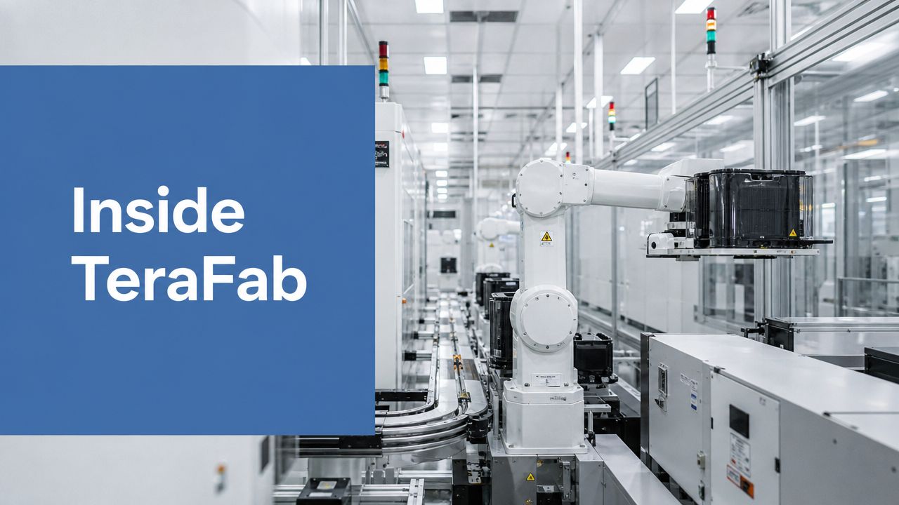
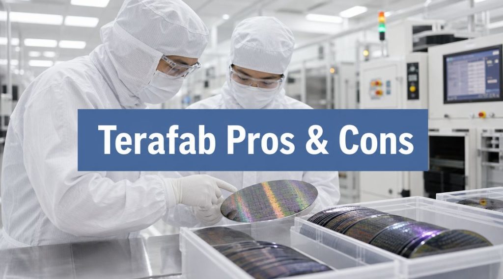
The image below captures that gap better than many headlines do.
Three risks dominate any serious assessment.
First, capital intensity. A vertically integrated semiconductor base presents a layered financing challenge that extends across land, construction, advanced tools, process development, packaging capacity, power, water, and long ramp periods before output becomes predictable. Even firms with large market values can struggle to fund projects that absorb cash for years while technical risk remains high.
Second, labor depth. Advanced fabs run on accumulated manufacturing experience, not general engineering prestige. Process integration leaders, lithography specialists, yield engineers, tool technicians, contamination experts, and factory operators are all in limited supply. Hiring them is only part of the task. Keeping them aligned through a difficult ramp is harder, especially when incumbent chipmakers already compete aggressively for the same people.
Third, ecosystem dependence. Vertical integration can reduce exposure to some outside suppliers, but it does not remove dependence on the semiconductor supply chain itself. Leading-edge production still relies on specialized equipment vendors, materials providers, packaging partners, software tools, and a network of tacit know-how built over decades. Any plan that implies near-total independence understates how interdependent this industry remains.
What Terafab reveals about market structure
Terafab is best understood as an extreme response to real pressures in the market.
AI infrastructure buyers want more control over cost, supply, and performance. Governments want domestic manufacturing capacity for strategic reasons. Large technology groups are rethinking whether reliance on a small set of external chip suppliers creates too much concentration risk.
Those pressures help explain why the concept keeps attracting attention. They do not make execution easier.
For investors, the useful distinction is between strategic coherence and delivery risk. Terafab can make sense as a response to bottlenecks in AI and advanced manufacturing while still looking financially and operationally daunting on the ground. That is the same discipline used in any sober assessment of whether a high-profile investment thesis carries outsized risk.
Broader Implications for the AI and Tech Industries
Ten questions serious readers still ask
A project like Terafab matters even if it never reaches its grandest public vision. It pushes the industry to reconsider what “normal” semiconductor structure should look like in an AI era.
Here are the questions that matter most.
- Is there a confirmed timeline? Public discussion centers more on ambition than on a fully transparent buildout schedule.
- Is this the same as a classic foundry strategy? No. The public framing is closer to a captive internal manufacturing system than a broad merchant foundry.
- How is this different from Intel's approach? Intel's public foundry identity has been tied to serving external customers. Terafab is discussed primarily as serving Musk-linked internal demand.
- Would it threaten Nvidia? Indirectly, if custom internal AI chips reduce reliance on outside accelerators. But that depends on execution, software, and volume.
- Could it affect TSMC? Strategically, yes, if major customers increasingly seek internal alternatives. Operationally, that's a much higher bar.
- What breakthroughs would matter most? Process maturity, packaging integration, and manufacturing consistency.
- Could others use Terafab? Current reporting points more toward internal use than broad outside access.
- Would it lower chip prices? Not automatically. Vertical integration can improve control, but it can also concentrate cost.
- How does it relate to Dojo and other in-house compute efforts? It looks like a manufacturing extension of the same desire for more stack control.
- Where would financing models evolve? Some founders looking at capital-heavy innovation study forms of startup funding without dilution, though a semiconductor project of this scale would still involve a far more complex capital structure.
What may change even if Terafab never reaches full vision
The biggest industry implication may be psychological. Terafab makes an aggressive claim that many firms have so far avoided making openly: for certain AI and robotics roadmaps, outsourced chip access may no longer feel sufficient.
That doesn't mean every company should imitate the model. Most shouldn't. The likely effect is more selective integration, more custom silicon programs, and more debate about where the clean break between software company and industrial company now sits.
The workforce side matters too. If advanced manufacturing and AI infrastructure continue converging, demand for hybrid talent will grow. That pressure already shows up across discussions of AI and automation reshaping the future workforce.
Frequently Asked Questions About Terafab
1. What does Terafab mean?
In current public reporting, Terafab refers to a planned vertically integrated semiconductor facility, not a generic technology term.
2. Is Terafab a real announced project or just an idea?
It has been publicly described as a project announced in Austin, Texas. The bigger debate is how much of the stated vision can be executed.
3. Is Terafab a foundry?
Not in the usual merchant-foundry sense. Reporting frames it more as an internal manufacturing system for Tesla, SpaceX, and xAI.
4. Why does vertical integration matter here?
Because it can reduce handoffs between design, fabrication, packaging, and testing, which may shorten iteration cycles and tighten process control.
5. Why are analysts skeptical?
Because advanced semiconductor manufacturing is expensive, talent-intensive, and dependent on a specialized global supply chain.
6. What makes the project unusual?
Its ambition. Public descriptions place it far outside the scale of a routine fab expansion.
7. Who would use the chips?
The concept is tied to internal demand from Tesla, SpaceX, and xAI rather than the broader open market.
8. Could Terafab compete with established leaders?
Only if it can solve cost, yield, and time-to-volume challenges that incumbent manufacturers have spent years mastering.
9. Is this mainly about AI?
AI is central, but the reported use cases also include autonomous vehicles, robotics, and space systems.
10. What's the smartest way to read Terafab news?
Treat it as both a strategic signal and an execution test. The vision is meaningful. The barriers are just as meaningful.
If you want more clear, evidence-first explainers on AI, industry, investing, and emerging tech, visit Everyday Next. It's a useful place to keep up with fast-moving topics without losing the practical context that makes them understandable.
Related Posts
Previous Post
Next Post