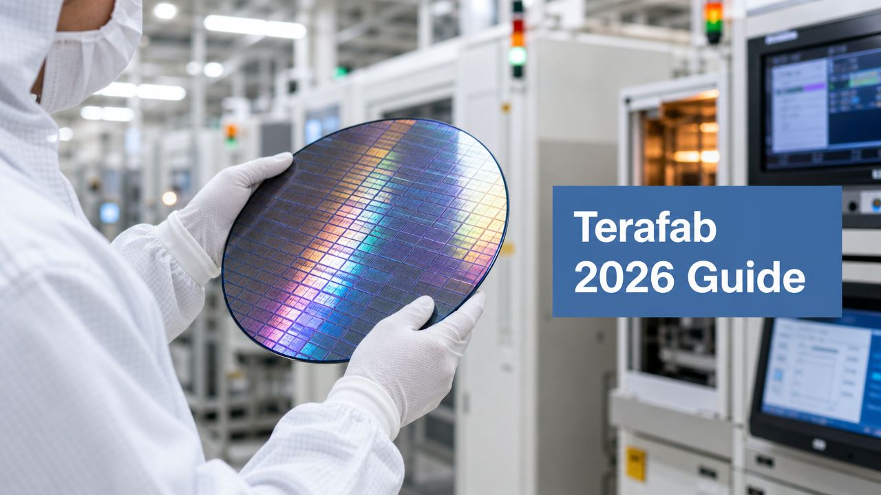
Terafab Pros and Cons Explained: A 2026 Analysis

1 month ago191 Views

A project can be visionary and still be physically implactical at its announced scale. Terafab sits in that uncomfortable middle ground. Public descriptions frame it as a facility designed to produce 1 terawatt of AI compute output annually, versus current global AI-chip output estimates of about 20 gigawatts per year, which is why supporters describe it as a roughly 50× leap if achieved, according to Fintech Weekly's summary of the plan.

That's the surprising part. The bigger the promise gets, the less useful a simple bullish or bearish take becomes. It's clear Terafab sounds ambitious; the useful question is whether any version of it can work, and what counts as success if the headline target never does. Readers tracking AI infrastructure, industrial policy, and capital-intensive tech bets should treat this as a feasibility story first, and a hype story second. For a broader look at the forces pushing these moonshot bets into the mainstream, this overview of top tech trends of 2025 gives helpful context.

Table of Contents

Introducing Terafab The Audacious Plan for AI Dominance

Terafab isn't being pitched like a normal semiconductor facility. It's being framed as a response to an AI hardware bottleneck, with one location combining chip design, fabrication, packaging, memory production, and testing. That structure matters because it would try to remove the handoff delays that slow most chip programs.

Robotic arms in an automated semiconductor manufacturing cleanroom for high-tech chip production and industrial automation.

The appeal is obvious. Tesla, xAI, and SpaceX all depend on specialized compute. A vertically integrated fab could, in theory, let them tune hardware for robotics, inference, and aerospace use cases without waiting in line behind larger foundry customers or coordinating across fragmented suppliers.

The credibility problem is just as obvious. The strongest outside analysis cited by Tom's Hardware argues that 1 terawatt of AI silicon per year would require roughly 142 to 358 fabs and well over $4 trillion in investment, compared with the publicly discussed $20 billion to $25 billion budget. That doesn't merely suggest difficulty. It raises a basic plausibility question.

The most useful way to read Terafab is not as a yes-or-no proposition. It's as a spectrum, from strategic niche success to industrial overreach.

That framing changes the analysis. If you read Terafab as an attempt to replace much of today's external supply structure, it looks extreme. If you read it as an attempt to secure critical in-house capacity for a few compute-hungry businesses, it starts to look less absurd and more like a high-risk industrial strategy.

What Is Terafab A Vertically Integrated Vision

Terafab is easiest to understand as a semiconductor version of an old manufacturing idea. Instead of relying on one company for design, another for wafer fabrication, another for packaging, and others for testing and memory, the project is described as pulling those functions into one ecosystem.

A diagram illustrating the Terafab concept as a vertically integrated vision for AI semiconductor development and production.

That's a radical departure from how the modern chip industry usually works. Most of the sector evolved toward specialization because each layer became too hard, too expensive, and too knowledge-intensive to master under one roof. Terafab's claim is that the strategic payoff of recombining those layers could outweigh the complexity.

A useful real-life analogy is Ford's River Rouge vision, where raw materials entered one side of the system and finished products came out the other. Terafab applies a similar logic to AI hardware. It wants less dependency, fewer bottlenecks, and tighter control over design-to-deployment decisions. For readers following automation trends, that logic overlaps with the broader rise in industrial robotics highlighted in this Everyday Next analysis of China's industrial robot production surge.

Three pillars define the concept

One pillar is massive scale. Public descriptions position Terafab around an output target far above current industry norms.

Another is vertical integration. The point isn't just making chips. It's owning more of the chain that turns chip ideas into deployed AI systems.

A third is strategic independence. For companies building custom AI products, supply assurance can matter as much as raw performance.

This visual captures the concept in one glance:

Why vertical integration matters

A conventional supply chain often creates friction at the boundaries.

Stage Traditional model Terafab vision
Design Separate design teams and outside manufacturing constraints Design closer to manufacturing realities
Fabrication Reliance on external foundry schedules Internal control over production priorities
Packaging and testing Additional vendors and logistics handoffs More consolidated iteration loop
Deployment fit General capacity allocation Tighter fit for internal product roadmaps

Practical rule: In semiconductors, control can be as valuable as capacity when the end product depends on custom hardware.

That's why Terafab gets attention. It isn't just another fab proposal. It's a proposal to collapse organizational distance between AI ambition and AI hardware production.

The Pros The Strategic Upside of Unprecedented Scale

Terafab's bullish case rests on a hard industry constraint: advanced AI companies are no longer limited mainly by ideas or even model talent. They are limited by access to enough compute, at the right time, on hardware tuned for their own workloads.

That shifts the strategic value of a fab proposal. The headline target matters because it implies an attempt to change bargaining power across the AI supply chain, not just add another manufacturing site. If even part of that capacity were directed internally, Tesla, SpaceX, and xAI could gain something more durable than short-term supply relief. They could reduce dependence on external foundry allocation cycles and align silicon roadmaps with product deadlines.

The strongest advantages show up at the portfolio level:

  • Priority access to scarce compute hardware: Internal programs would not be queued behind the broader customer base of a third-party foundry.
  • Faster design-to-deployment cycles: Closer coordination between chip teams, packaging, systems engineering, and end-product groups can shorten iteration loops.
  • Workload-specific silicon economics: Custom chips make more sense when the buyer also controls the software stack, deployment environment, and volume demand.
  • Strategic insulation: A company with internal capacity is less exposed to supplier concentration risk, pricing pressure, and geopolitical disruption. Investors trying to discover market risk strategies will recognize why that matters.

The last point is easy to underrate. Foundry dependence is not only a procurement issue. It shapes product timing, feature scope, and capital planning. For firms building autonomy systems, robotics, launch infrastructure, or large model services, delayed hardware can postpone revenue, model training, or fleet rollouts by quarters.

That is why a partial success case deserves more attention than the all-or-nothing version usually discussed.

Terafab does not need to reach its full stated ambition to matter commercially. A narrower outcome, such as reliable internal production for a subset of accelerators, advanced packaging, or specialized inference chips, could still improve margins and planning discipline for high-priority programs. Tesla could use that for autonomy and robotics. xAI could use it for training or inference bottlenecks. SpaceX could use it where system reliability and supply assurance matter more than chasing the absolute leading edge.

Potential upside Why it matters
Dedicated internal capacity Lowers exposure to external allocation decisions and supply shocks
Better packaging and memory coordination Improves performance per system, not just per chip
Tighter product timing Links chip availability more closely to software, vehicle, robotics, and AI service launches

There is also a second-order effect. If Terafab produced even moderate internal capacity, it could give these companies more negotiating power with outside suppliers. Owning part of the stack changes commercial relationships across the rest of the stack.

That makes Terafab financially interesting even below the headline vision. Full terawatt-scale execution strains physical and capital realities, but partial vertical integration could still create a meaningful edge in the parts of AI where hardware-software co-design matters most. That broader shift toward purpose-built systems is already visible in real-world generative AI business applications across industries.

The realistic upside is not “own the entire future of AI chips.” It is gaining enough internal manufacturing and packaging control to improve product velocity, reduce dependency risk, and strengthen economics in a few very large businesses.

The Cons The Immense Risks and Feasibility Hurdles

Terafab's hardest problem is not ambition. It is manufacturing credibility.

A 1 terawatt vision collides with an industry that punishes inexperience more harshly than most capital markets models do. Building advanced semiconductor capacity requires more than money and executive will. It requires years of process learning, supplier coordination, yield improvement, packaging discipline, and a workforce that has already solved similar problems under production conditions. As noted earlier, public reporting has also framed the project around very high capital needs and a long ramp, which matters because time is often the scarcest input in semiconductors.

A comparison chart outlining the major risks and potential benefits for the Terafab project initiative.

Execution is the central problem

The core risk is cumulative. Terafab is not trying to master one difficult layer of the stack. It appears to be attempting several at once, including chip design coordination, foundry relationships, packaging, infrastructure, and downstream system integration. Each layer can slip independently. Delays then cascade into the others.

Reporting from TradingKey highlights that broad scope, aggressive timing, staffing limits, and dependence on Intel's 14A process could all become chokepoints. That last point deserves more attention than it usually gets. A vertically integrated story still depends on external roadmaps if core process technology sits outside the company's direct control. In practice, that means Terafab may be less vertically integrated than the branding suggests.

Three constraints matter most:

  • Equipment availability: Advanced tools often have long procurement cycles, which can push schedules even with committed funding.
  • Facility precision: Leading-edge production depends on contamination control, vibration management, power quality, and water systems that leave little room for error.
  • Manufacturing learning curves: Designing a chip and producing it at commercially useful yields are separate challenges.

This is why partial success deserves serious attention. If Terafab falls well short of the headline target but still secures better packaging control, dedicated capacity, or tighter integration for Tesla and SpaceX workloads, it could still produce strategic value. The downside is that investors may price the project as if scale and execution are a package deal, when they are not.

Why budget alone does not solve the problem

Large budgets often hide the actual bottleneck. Semiconductor projects fail less often from lack of ambition than from the difficulty of aligning process technology, supply chains, talent, validation, and end-market timing.

A practical way to assess Terafab is to separate capital risk, timeline risk, and capability risk. If you want a simple primer on how professionals discover market risk strategies, that framing is useful here too. Terafab concentrates all three in one initiative, which raises the odds that one delay or cost overrun changes the economics of the whole program.

There is also a geopolitical layer that hype-heavy coverage often misses. Even an internally focused fab remains exposed to foreign equipment vendors, specialty materials, export controls, and shifting trade policy. That exposure becomes more important if the business case assumes predictable access to tools and components over many years, which is why the broader context in this analysis of 2025 tariff and trade shifts matters.

The non-obvious conclusion is straightforward. Terafab does not need to fail outright to disappoint. It only needs to arrive late, cost more than expected, or deliver less manufacturing independence than the narrative implies. In semiconductors, those outcomes are common, and they are enough to turn a grand strategic thesis into a narrower, more expensive partial win.

How Terafab Compares to Traditional Chip Fabs

Most chip manufacturing models became specialized for a reason. TSMC represents the pure-play foundry approach. Intel represents the classic integrated device manufacturer approach. Terafab, as described publicly, goes further than either by trying to combine broad in-house control with a mission-specific AI ecosystem.

A comparison chart showing differences in business models and focus between Terafab, TSMC, and Intel chip fabrication.

A different model from TSMC and Intel

TSMC's strength comes from focus. It manufactures for many customers and invests significantly in process technology. Intel's traditional model combines design and manufacturing, but within a company built around semiconductor operations.

Terafab proposes something different. It would serve a narrow set of affiliated companies while also trying to integrate more of the stack around AI-specific needs. That can be powerful if the workloads are unique enough. It can also be dangerous because it rejects the industry's longstanding preference for specialization.

There's also an infrastructure problem that traditional fabs don't confront at this scale. Coverage of the project says the 1 terawatt per year target would require more electricity than major national power systems, and that a large share of output would theoretically need to be sent off-planet because Earth-side energy and infrastructure limits couldn't support all intended deployment, according to this project discussion on YouTube. That puts Terafab in a category beyond normal fab comparison.

For context on where AI compute demand may be heading inside enterprises, this Everyday Next article on Jensen Huang's view of AI agents helps show why companies keep chasing deeper hardware control.

Comparison table

Feature Terafab TSMC Intel
Core model Vertically integrated AI-focused ecosystem Pure-play foundry Integrated device manufacturer
Customer base Primarily affiliated internal demand Broad external customer base Historically internal products plus foundry ambitions
Main promise End-to-end control and optimization Manufacturing specialization and scale Integrated design-manufacturing heritage
Main weakness Extreme execution complexity Less control for customers over full stack Balancing product strategy with manufacturing execution
Best-case role Strategic in-house AI supply engine Global manufacturing backbone Hybrid design and manufacturing platform

The comparison isn't who is “better.” It's which model best fits the problem being solved. TSMC optimizes for broad industrial service. Intel optimizes around a semiconductor company's own product and process ambitions. Terafab would optimize around control for a concentrated AI empire.

Ideal Use Cases and The Realistic Market Impact

The most grounded way to evaluate Terafab is to stop treating it as an all-or-nothing bet. If it never reaches the headline vision, it could still matter if it creates a reliable internal pipeline for a few high-stakes products. That's the practical angle often missing from terafab pros and cons explained pieces.

According to Teslarati's summary of the project debate, the global industry produces about 20 gigawatts of computing capacity annually, while the strategic value for investors may lie less in trying to match outside foundries on sheer volume and more in Terafab's ability to provide partial vertical integration for Tesla, SpaceX, and xAI mission-critical custom chips.

Where partial success could still matter

A smaller but capable fab could still be strategically valuable in areas where delay is expensive and substitution is hard.

Three use cases stand out:

  • Tesla robotics and autonomy: Custom chips for Optimus or vehicle inference don't have to dominate the global market to matter. They need dependable supply and tight software-hardware fit.
  • xAI inference and training adjacencies: A dedicated internal path for specialized AI silicon could help align model architecture with hardware constraints.
  • SpaceX and orbital compute: Mission-specific compute has different reliability and deployment pressures than generic cloud demand.

The market may eventually judge Terafab less by its maximum output target and more by whether it lowers supply risk for the workloads Musk's companies can't easily outsource.

Real life examples of strategic fit

A useful real-life comparison is not another fab announcement. It's the broader pattern of companies bringing critical inputs in-house when outside markets become too constrained or too generic for their needs.

Real-world pattern Relevance to Terafab
Car makers investing deeper into battery supply chains Control over a strategic input can matter more than lowest unit cost
Cloud providers developing custom AI chips Tailored silicon can outperform generic procurement for defined workloads
Aerospace firms insisting on tightly controlled components Reliability and mission fit often outweigh broad market flexibility

That's why a “partial success” scenario deserves more attention. If Terafab evolves into a smaller advanced fab, strong in packaging, memory integration, and internal custom chip programs, it could still generate a strategic advantage. It wouldn't need to displace TSMC. It would need to make Tesla, xAI, and SpaceX less exposed to external bottlenecks.

For investors, that shifts the scorecard. The relevant question becomes whether Terafab can build a strategic moat around niche but high-value compute demand. If it can, the project may matter even as the original scale target remains aspirational.

Frequently Asked Questions About Terafab

1. What is Terafab in simple terms?

Terafab is a proposed chip manufacturing complex that aims to pull several hard-to-coordinate functions into one system, including chip design, fabrication, advanced packaging, memory-related processes, testing, and deployment for affiliated companies.

The ambition matters because each of those steps is usually split across specialized firms, geographies, and long supplier timelines.

2. Why are people paying so much attention to it?

Because the proposal is unusually large in both physical scope and strategic intent. It is being discussed less as a standard fab project and more as an attempt to secure computing capacity for Tesla, xAI, and SpaceX at a time when advanced AI hardware has become a bottleneck.

That framing pushes the debate beyond technology. It raises questions about capital intensity, industrial execution, and whether internal control is worth more than buying from established suppliers.

3. What is the main advantage of Terafab?

The clearest upside is tighter control over a constrained input. If one organization can align chip design, packaging, testing, and deployment around its own workloads, it may shorten iteration cycles and reduce exposure to outside shortages.

For companies building large AI systems, autonomous platforms, and mission-specific hardware, that control can have strategic value even if unit economics are not best-in-class.

4. What is the biggest risk?

Execution risk is still the center of the case against Terafab. Advanced semiconductor production depends on process knowledge, equipment coordination, yield management, and supplier relationships that usually take years to build.

That is why skepticism is not just about ambition. It is about whether a new entrant can translate money and urgency into reliable manufacturing output.

5. How much is Terafab expected to cost?

Public estimates discussed earlier in this article place the project in the tens of billions of dollars. The exact number matters less than the underlying point. Even a scaled-down version would demand very large capital commitments before proving it can operate efficiently.

In semiconductors, construction is only the opening expense. Tooling, ramp time, engineering talent, process learning, and yield improvement can keep absorbing capital long after the facility is built.

6. Can a new fab really be built quickly?

A building can go up faster than a manufacturing operation can mature. The hard part is not pouring concrete. It is getting complex production lines to run consistently, at acceptable yields, with repeatable quality.

That distinction gets lost in headline timelines.

7. Is the 1 terawatt target realistic?

It looks highly speculative based on the constraints already discussed in this article. Reaching that scale would require far more than a single successful facility. It would imply extraordinary access to power, equipment, process expertise, and capital over multiple years.

A better question is what happens if the target is missed by a wide margin. Partial success could still matter if Terafab becomes a credible internal source of advanced packaging, custom silicon support, or specialized compute capacity.

8. How is Terafab different from TSMC?

TSMC operates as a specialized foundry serving a broad customer base across the industry. Terafab is being described as a vertically integrated, mission-driven manufacturing system oriented around the needs of a small set of affiliated companies.

That difference has consequences. A broad foundry can spread cost, learning, and demand across many customers. A captive or semi-captive system gets tighter alignment, but it also carries more concentration risk if internal demand shifts or execution slips.

9. Could Terafab still matter if it never hits the headline goal?

Yes. This is one of the most plausible outcomes.

If the project ends up smaller than advertised but still useful, it could reduce dependence on external suppliers for selected high-value workloads. That would be meaningful for Tesla's robotics and autonomy programs, for SpaceX systems that need tighter component control, and for AI training or inference stacks that benefit from custom packaging and integration.

In that scenario, Terafab would not need to remake the semiconductor industry to justify itself. It would need to improve supply certainty for a narrow set of expensive, strategically important compute needs.

10. What should investors watch most closely?

Watch operating evidence, not narrative momentum. The best signals would be hiring of experienced semiconductor operators, credible partnerships in tooling and process development, realistic phasing of construction and ramp plans, and proof that the project can produce useful output before any extreme scale target is approached.

Investors should also watch for a shift in how success is defined. If management starts emphasizing packaging, custom accelerators, or internal supply resilience over the original terawatt ambition, that may reflect realism rather than failure.


If you like deep, evidence-based breakdowns of ambitious tech and investment stories, Everyday Next is worth bookmarking. It regularly covers AI, innovation, markets, and practical explainers for readers who want clarity instead of hype.

Leave a reply

Follow
Sidebar Search Add a link / post
Popular
Loading

Signing-in 3 seconds...

Signing-up 3 seconds...