Inside TeraFab Factory Design: A 2026 Analysis
A semiconductor project aiming for 1 million wafer starts per month and a campus of about 100 million square feet isn't just another fab proposal. It's a claim that the standard semiconductor production model may be too slow, too fragmented, and too exposed to outside bottlenecks for the AI era to tolerate (public project description).
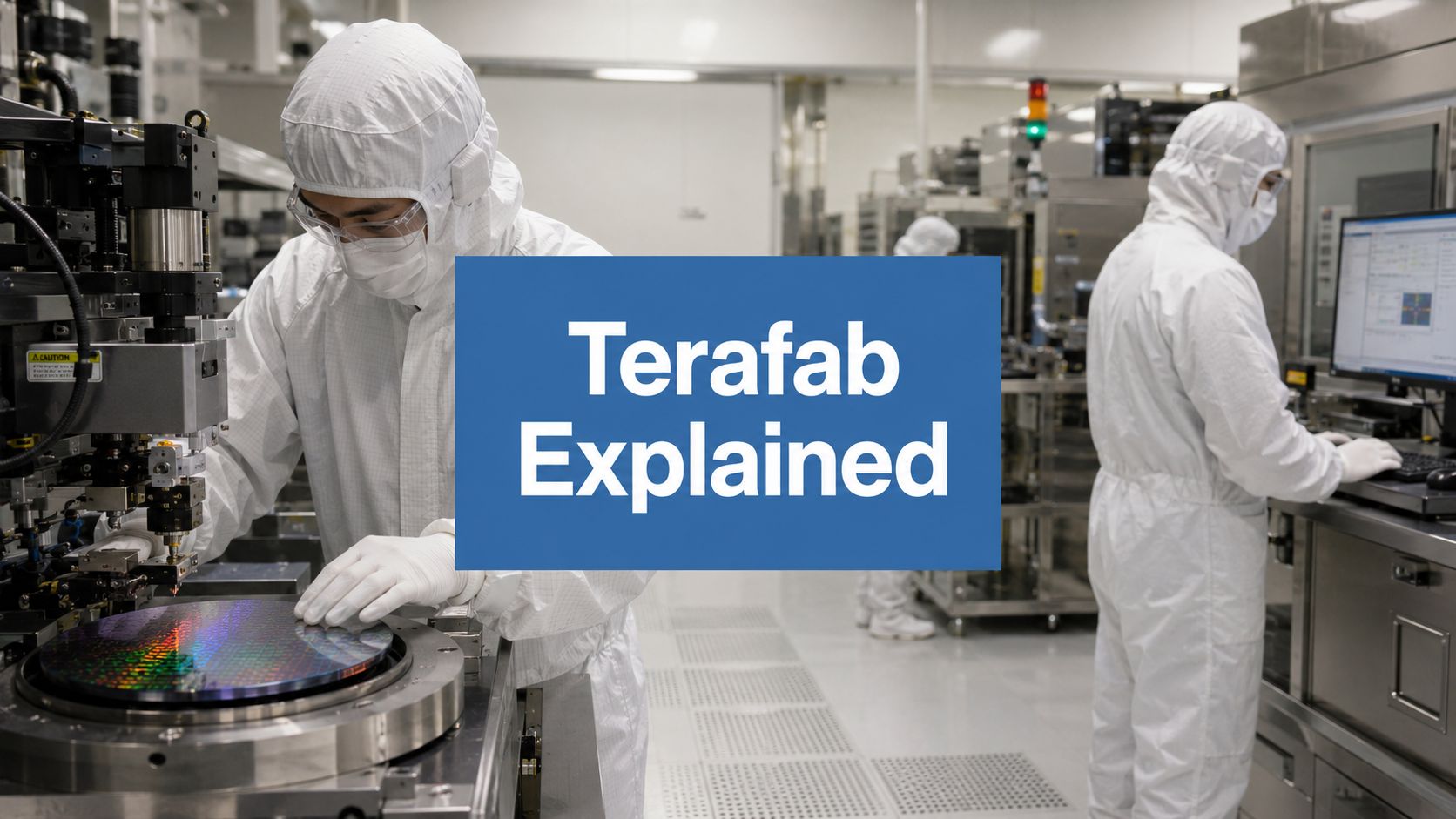
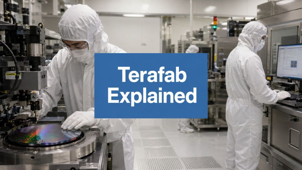
That's the right way to read inside TeraFab factory design. Not as a building story, but as a systems story. If the public descriptions hold, TeraFab is an attempt to collapse design, lithography, fabrication, memory production, advanced packaging, testing, and mask production into a single industrial loop in Austin. For investors and operators, that changes the question from “Can they build a fab?” to “Can one campus reorganize the economics and speed of AI hardware production?”
Table of Contents
- What Is TeraFab and Why It Changes Everything
- The Core Concept of Vertical Integration
- Designing for a Million Wafers per Month
- The Technology Stack and Automation
- Decoding the Economics of TeraFab
- Strategic Implications for Business and Investment
- Frequently Asked Questions About TeraFab
- 1. Is TeraFab a real announced project or just rumor?
- 2. What makes TeraFab different from a standard semiconductor fab?
- 3. Why is vertical integration so important here?
- 4. Is the one million wafer target realistic?
- 5. Who are the intended chip customers?
- 6. Why does the campus size matter so much?
- 7. What is the role of the research fab?
- 8. Could TeraFab threaten established foundries?
- 9. What is the biggest execution risk?
- 10. What should investors watch first?
What Is TeraFab and Why It Changes Everything
A semiconductor campus proposed at roughly 100 million square feet and aimed at 1 million wafer starts per month is not a routine fab expansion. Those figures point to a different industrial model altogether. As described publicly, TeraFab is a Texas-based project intended to combine major chipmaking functions for two distinct product tracks: chips for terrestrial systems such as vehicles and humanoid robots, and radiation-hardened devices for space use.
The important point is not the headline scale by itself. It is the combination of scale and scope. A conventional fab is one piece of a distributed supply chain, with design, manufacturing, packaging, and test often split across separate companies and regions. TeraFab, based on its public concept, aims to compress those functions into one operating environment.
For investors, that changes the frame from factory economics to platform economics.
If the model works, the benefit is not limited to higher output. It can reduce coordination delays, shorten engineering feedback loops, and shift more of the value chain inside a single corporate boundary. That is a familiar logic in batteries and vehicles. Applied to semiconductors, it carries larger implications because chip programs are constrained not only by capital intensity, but also by cycle time and packaging bottlenecks.
Why investors should view it as infrastructure
AI hardware demand has exposed a weak point in the traditional semiconductor model. Design teams can move quickly, while manufacturing, packaging, and test move on separate calendars and often under separate incentives. A vertically integrated campus addresses that mismatch by turning external handoffs into internal process control.
That strategic choice matters more than the factory rendering.
The strongest comparison is not to a larger merchant foundry. It is to an integrated production system built for a captive set of end products. That distinction affects margins, supply assurance, and product timing. A merchant foundry maximizes utilization across many customers. An integrated operator can instead optimize for its own roadmap, its own packaging choices, and its own demand spikes.
Readers following broader shifts toward tightly coupled hardware and software stacks can place TeraFab within the same pattern seen across top tech trends of 2025. The common theme is tighter control over bottlenecks that used to sit outside the company.
Why the public numbers matter more than they first appear
The headline metrics imply a competitive doctrine, not just ambition on paper.
- Control over supply reduces exposure to third-party capacity shortages.
- Control over iteration can shorten the time between a design issue, a process change, and the next production run.
- Control over end-market fit allows chips to be designed for internal systems such as vehicles, robotics, and space hardware rather than generalized for outside customers.
The third point is easy to underestimate. Merchant foundries are designed to serve a broad customer base, which pushes them toward standardization. A vertically integrated campus can justify narrower optimization if the downstream products are large enough and strategically important enough. In that scenario, the payoff is not just more wafers. It is greater freedom to choose architectures, packaging methods, and release schedules without waiting on the priorities of external suppliers.
The Core Concept of Vertical Integration
The semiconductor industry usually works through separation. One group designs chips. Another runs the fab. Another handles packaging. Another performs testing. The system works, but it creates friction at every handoff.
TeraFab's public design breaks with that model by combining chip design, fabrication, memory production, advanced packaging, and testing on a single campus, with the stated aim of drastically shortening the feedback loop between design and manufacturing (integrated campus description).

Why this model is different from standard chipmaking
A fragmented model can still produce world-class chips. The problem is that every transfer creates delay, translation risk, and inventory exposure. Designers may discover a manufacturability issue late. Packaging constraints may arrive after architecture decisions. Test data may return too slowly to affect the next revision.
A single-campus model changes the cadence.
- Design teams can work closer to process constraints.
- Manufacturing teams can push direct feedback into the next tapeout cycle.
- Packaging and test groups can expose bottlenecks before they become product delays.
This doesn't guarantee better results. It does create the conditions for faster learning.
The River Rouge analogy still fits
The cleanest historical comparison isn't another modern fab. It's Ford's River Rouge complex, where raw materials and finished products sat in one industrial chain. TeraFab appears to borrow that logic for semiconductors. Instead of accepting the modern industry's specialization as fixed, it asks whether strategic control is worth reassembling the chain.
Vertical integration doesn't remove technical difficulty. It relocates coordination from contracts and suppliers into one management system.
That tradeoff matters for security and resilience too. A fragmented semiconductor chain is exposed to transport risk, supplier prioritization, and geopolitical disruption. A single-campus approach can't eliminate those risks entirely, but it can shrink the number of external dependencies between concept and finished device.
What the design says about management priorities
Inside TeraFab factory design, the clearest signal isn't the building size. It's the choice to put adjacent stages of the value chain under one operating structure. That suggests management is prioritizing speed of iteration, supply assurance, and product-specific optimization over the flexibility of outsourcing.
For investors, that points to a simple but important conclusion. If the project succeeds, its advantage may show up first in cycle time and product coordination, not just in unit economics. In semiconductors, faster learning can become a bigger moat than lower price.
Designing for a Million Wafers per Month
A target of 1 million wafer starts per month sits far outside the range usually discussed for a leading-edge logic fab. Tom's Hardware notes that modern advanced fabs are typically measured in the tens of thousands of wafer starts per month, not seven figures (scale comparison). For investors, that gap matters because it changes the design question from "how large is the fab?" to "what operating model could sustain output at that scale without collapsing yield or utilization?"
A conventional fab blueprint does not scale linearly to that level. More floor area helps, but it does not solve the coordination burden created when thousands of process steps, tool states, material movements, and maintenance windows must stay synchronized across a very large site. The more plausible interpretation is a campus built from repeated production modules, each standardized enough to replicate, but isolated enough that one interruption does not drag the whole system off schedule.
Why a conventional fab blueprint won't work
At ordinary fab scale, management can still concentrate on optimizing one tightly controlled line. At TeraFab scale, the binding constraint shifts toward system design. Throughput depends on whether the campus can absorb tool downtime, qualification delays, and process drift without creating long queues at a few expensive bottlenecks.
That has direct business implications. A modular layout would require more upfront discipline in tool matching, process transfer, and software control, but it could also reduce execution risk compared with one giant, tightly coupled line. Hyperscale data center operators learned this years ago. Repeatable blocks are easier to expand, maintain, and finance than a one-off structure whose economics depend on every subsystem staying perfectly aligned.
| Metric | Conventional Leading-Edge Fab | TeraFab Target Full Scale |
|---|---|---|
| Wafer starts per month | 20,000 to 30,000 | 1 million |
| Campus structure | Usually a single major fab line with support functions | Likely a modular multi-fab campus operating in parallel |
| Design implication | Optimize one facility for consistency | Coordinate many production cells without losing yield discipline |
Beyond footprint, the core challenge is flow
Square footage gets attention because it is easy to visualize. Flow determines whether the project works.
Wafers, reticles, chemicals, spare parts, and finished devices have to move through controlled environments with minimal delay and minimal contamination risk. As volume rises, transport distance, handoff frequency, queue time, and dispatch accuracy start to influence economics almost as much as the process technology itself. A layout that adds a few minutes of friction to thousands of lots can gradually consume capacity that looked available on paper.
That is why path design matters so much. Operators at this scale would need routines that boost manufacturing productivity through tighter scheduling, faster exception handling, and fewer hidden idle intervals between tools. In semiconductors, those disciplines do more than improve labor efficiency. They protect cycle time and help contain yield loss that can spread when lots sit too long or arrive out of sequence.
Practical rule: At extreme wafer volume, the winning factory is the one that keeps bottleneck tools continuously fed without creating instability elsewhere in the line.
Why software architecture becomes part of factory architecture
A campus intended to operate like many fabs at once cannot rely on local decisions alone. It needs central visibility over dispatch, maintenance, and lot priority, while giving individual modules enough autonomy to keep running when one area falls behind. Physical design and software design therefore become one investment decision, not two separate ones.
TeraFab's vertical integration thesis becomes more concrete: If the company controls adjacent stages of design, manufacturing, and downstream product use, it can tune factory logic around its own demand patterns rather than around the broader merchant foundry market. That could improve cycle-time predictability for internal programs, but it also raises the execution bar. The software layer has to coordinate a campus that behaves more like distributed infrastructure than a single plant, which is why the tradeoffs discussed in cloud computing benefits and drawbacks are relevant here too. Centralized control offers visibility and consistency, but only if latency, resilience, and trust remain strong at the tool level.
For savvy investors, that leads to a less obvious conclusion. The design challenge is not mainly whether TeraFab can build a very large fab. It is whether it can standardize a repeatable manufacturing system that compounds learning across modules faster than complexity compounds failure. If that works, the advantage would extend beyond capacity. It would create a template for scaling semiconductor production more like compute infrastructure, which would be a meaningful break from established fab economics.
The Technology Stack and Automation
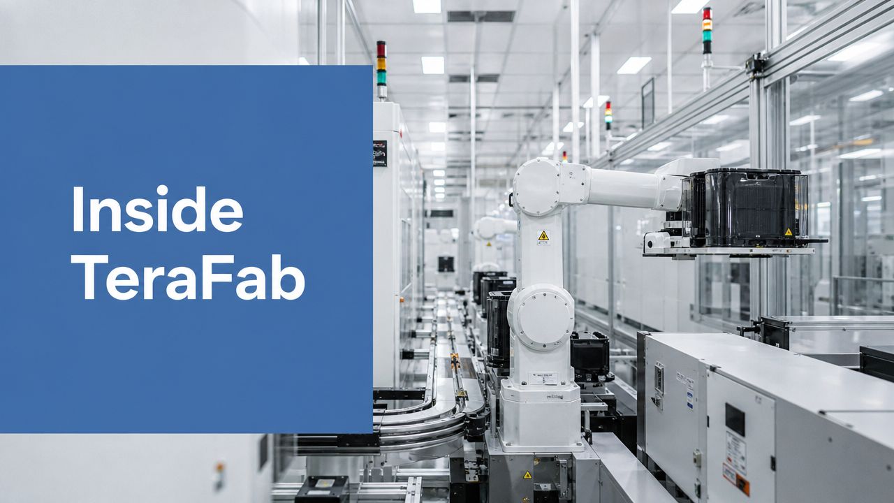
A factory with this kind of complexity won't be managed by headcount alone. It needs a software layer that acts like a nervous system, continuously translating design priorities into equipment actions, maintenance decisions, transport scheduling, and yield controls.

The public descriptions of TeraFab emphasize vertical integration. In practice, that only works if the software stack is integrated too. A fragmented digital layer would recreate the same delays that a single-campus model is supposed to remove.
What automation would need to do
For a site this ambitious, automation isn't mainly about replacing labor. It's about coordinating thousands of decisions that humans can't make fast enough or consistently enough at full scale.
A plausible stack would need to handle:
- Material handling: moving wafers, masks, and components between tightly controlled stages.
- Yield monitoring: spotting process drift before it spreads across more lots.
- Tool scheduling: prioritizing expensive bottleneck equipment with minimal idle time.
- Maintenance timing: intervening before failures stop production.
One accessible explanation of why this matters comes from industrial maintenance practice. Predictive maintenance works because it shifts operations away from reacting to breakdowns and toward detecting early signs of trouble. That logic is relevant here, and this overview from Wilcox Door Service Inc. is a useful non-semiconductor primer on the concept.
The digital twin becomes a management necessity
The term “digital twin” gets overused, but in a campus this large it has a concrete meaning. Operators would need a live digital model of the facility that connects equipment status, process conditions, work in progress, and quality signals. Without that, managers are flying blind between local dashboards.
A true digital twin would let teams test routing changes, identify emerging bottlenecks, and evaluate the ripple effects of taking tools offline. In a vertically integrated environment, it could also connect downstream packaging and testing results back to upstream process choices.
The broader industrial context matters. Advanced manufacturing is moving toward more robotized and sensor-driven operations, and that trend is part of the same shift described in this report on China's industrial robot production surge.
Here's a useful visual reference for how industrial automation environments are increasingly presented and discussed:
Why unified software may be the hidden differentiator
Investors often focus on lithography tools, process nodes, and capital budgets. Those matter. But for a speculative project like TeraFab, the hidden differentiator may be software coherence.
A campus can buy advanced machines and still fail if its planning, maintenance, quality, and logistics systems don't speak the same language.
Inside TeraFab factory design, automation is the part that turns vertical integration from a slogan into a workflow. If one system can see design intent, production status, and downstream quality at once, the factory starts to behave less like a collection of departments and more like a coordinated organism. That's where the strategic payoff begins.
Decoding the Economics of TeraFab
A leading-edge fab can absorb tens of billions in capital before it proves a single long-term margin assumption. That is why TeraFab should be assessed less as a construction story and more as a capital allocation test.

The economic case hinges on sequence. As noted earlier, public discussion describes an initial research-oriented fab at Giga Texas before any full campus-scale rollout. For investors, that matters more than the largest headline figure because phased capacity changes the decision tree. Management is not only buying equipment. It is buying information about yield, integration difficulty, packaging flow, and software coordination before committing to the hardest scaling step.
Why the pilot stage matters financially
Pilot fabs rarely look attractive on stand-alone return metrics. Their value comes from reducing the probability of a much larger mistake.
That distinction is easy to miss in speculative projects. A smaller facility can expose whether process modules work together, whether internal packaging assumptions hold up, and whether operating software can coordinate the factory at useful speed. If those answers are negative, losses are contained. If they are positive, the pilot does more than validate technology. It improves the odds that later capital is deployed into a system that can ramp effectively.
For a conventional foundry, that learning is spread across many customers and product families. TeraFab appears to be framed around concentrated internal demand. That changes the economics.
Internal demand changes the threshold for acceptable returns
A merchant fab has to maximize utilization across external customers with different designs, timelines, and margin profiles. An integrated operator can accept a different payoff structure if the fab protects a larger product stack.
The practical question is not whether wafer output alone beats outsourced pricing in year one. The practical question is whether in-house manufacturing lowers total system cost across vehicles, robotics, and compute hardware over several product cycles. That includes effects that standard fab models often understate:
- Supplier margin capture: manufacturing value that would sit with external partners stays inside the corporate structure.
- Faster iteration: process changes and design revisions can be coordinated against product launch schedules instead of vendor queues.
- Roadmap control: silicon choices can be matched to internal hardware priorities rather than to the broader customer mix of a foundry.
Owning fabrication capacity can look expensive on a fab P&L and still make strategic sense if it prevents delays or design compromises in much larger end markets.
This is the key analytical difference between TeraFab and a normal semiconductor expansion. The asset may be justified by downstream economics, not just semiconductor margins. If Tesla or SpaceX view chips as rate-limiting components for vehicles, autonomy systems, robots, or space hardware, then the fab becomes part of product strategy, not just manufacturing overhead.
What would make the model work
Scale by itself does not create acceptable returns. Learning velocity does.
A vertically integrated fab starts to earn its keep when each process cycle improves more than one part of the business at once. Better yields reduce unit cost. Better packaging alignment improves system performance. Better scheduling shortens product release timelines. Those gains are correlated, which is why some integrated models can outperform what a line-item cost comparison would suggest.
The same logic applies to energy and facility design. Large industrial campuses face rising pressure to show they can improve throughput without locking in inefficient resource use. That broader constraint is part of the case for sustainability-driven industrial design choices, especially for projects that will be judged over decades rather than quarters.
What investors should actually monitor
Headline capex is the least interesting metric after the initial announcement. Three operating signals matter more.
| Decision area | Why it matters |
|---|---|
| Pilot-to-scale conversion | Shows whether the early fab is generating usable process and operating knowledge, not just publicity |
| Yield and packaging consistency | Indicates whether vertical integration is producing compounding learning across fabrication and downstream assembly |
| Product fit across internal programs | Tests whether fab output is aligned with the chip requirements of vehicles, robotics, and other in-house systems |
The investment implication is straightforward. TeraFab only becomes economically persuasive if it turns fixed cost into a timing advantage, a design advantage, or both. If it does, the project would challenge a core industry assumption: that outsourcing remains the default best option even for companies with very large, highly specific silicon demand. If it does not, the result is a very expensive reminder that semiconductor integration punishes execution errors at scale.
Strategic Implications for Business and Investment
The strategic significance of TeraFab comes down to one question. What happens if a major AI hardware consumer stops behaving like a normal customer and starts behaving like a fully integrated semiconductor platform?
For Tesla and SpaceX, the answer is straightforward. If they can pair in-house chip design with in-house manufacturing and packaging, they gain tighter control over cost, timing, and product specialization. That could matter more for fast-moving systems like vehicles, robotics, and space hardware than it would for a slower, broader electronics business.
What this means for the semiconductor model
TeraFab doesn't automatically replace the fabless-foundry model. That model exists for good reasons. It spreads risk, pools demand, and allows specialists to dominate different parts of the chain.
But a project like this challenges one assumption behind that model. It suggests that for a company with large enough internal demand and narrow enough product focus, outsourcing may no longer be the optimal default. If TeraFab demonstrates that vertical integration shortens learning loops and protects strategic supply, other AI-intensive firms may rethink how much silicon control they need.
The investor lens should stay balanced
Enthusiasm must be tempered by discipline. The upside case is large because the strategic goal is large. A successful TeraFab could create a serious moat around custom AI hardware and reduce dependence on outside manufacturing priorities.
The risk case is also large. Semiconductor production is unforgiving. Building a vertically integrated campus doesn't just require money. It requires process mastery, software discipline, operational consistency, and management patience. Failure can occur in any one of those layers.
Investors shouldn't ask whether TeraFab sounds visionary. They should ask whether the organization can convert vertical integration into repeatable operating advantage.
A practical framework for evaluating projects like this
For savvy investors and tech professionals, inside TeraFab factory design is most useful as a template for evaluating a new class of industrial bets.
- Is there real internal demand? A giant fab without a clear product pull is just capex.
- Does integration solve a known bottleneck? If not, complexity may outweigh control.
- Can software unify the operation? Without that, the campus becomes a collection of expensive silos.
That same framework is increasingly relevant across advanced industry, where AI and automation are reshaping the future workforce. TeraFab sits at the sharp end of that shift. It treats manufacturing, software, and product strategy as one combined system. If that works, competitors won't just need better chips. They'll need a better operating model.
Frequently Asked Questions About TeraFab
1. Is TeraFab a real announced project or just rumor?
Public descriptions say TeraFab was announced on March 21, 2026 as a vertically integrated semiconductor facility in Austin, Texas. What remains uncertain is how much of the final vision is fixed versus still evolving in public discussion.
2. What makes TeraFab different from a standard semiconductor fab?
The defining difference is integration. Public descriptions present TeraFab as combining design, fabrication, memory production, advanced packaging, testing, and mask production in one campus rather than splitting those functions across multiple suppliers.
3. Why is vertical integration so important here?
Because semiconductors often slow down at organizational boundaries. When design, fab, packaging, and test sit apart, delays and misalignment accumulate. TeraFab's model tries to pull those handoffs into one operating loop.
4. Is the one million wafer target realistic?
It's a public target, not a proven operating result. The main takeaway isn't certainty that it will be reached. It's that the target implies a modular multi-fab campus, not a conventional single-fab design.
5. Who are the intended chip customers?
Public descriptions tie the output to two main chip families. One is for terrestrial products such as Tesla vehicles and Optimus robots. The other is a radiation-hardened design for space applications.
6. Why does the campus size matter so much?
Because the physical footprint signals the ambition to combine many manufacturing stages and massive throughput in one location. Size here reflects process integration, not just real estate.
7. What is the role of the research fab?
Public discussion points to a smaller research fab at Giga Texas intended to test ideas before larger-scale production. That matters because it creates a pilot stage for learning before full deployment.
8. Could TeraFab threaten established foundries?
Not immediately in the broad market sense. But it could challenge the assumption that every major AI hardware buyer should stay dependent on external foundries for its most strategic silicon.
9. What is the biggest execution risk?
Coordination. Leading-edge manufacturing already demands precision. A vertically integrated mega-campus adds another layer of complexity because many specialized functions must work as one system.
10. What should investors watch first?
Watch for evidence that the pilot approach produces real operational learning, that automation and software integration are coherent, and that product roadmaps stay aligned with manufacturing plans. Those signals matter more than headlines alone.
Everyday Next publishes practical analysis for readers who want clear thinking on technology, investing, and industry shifts. If you want more breakdowns like this one, follow Everyday Next for explainers that connect big ideas to real business implications.
Related Posts
Previous Post
Next Post