How Big Is Terafab Project: 2026 Scale Explained
You’ve probably heard the buzz around Elon Musk’s Terafab project. It’s a huge, self-sufficient semiconductor super-factory, a massive joint effort between Tesla, SpaceX, and xAI. But when people ask "how big is it?", the numbers are almost hard to believe.
The quick answer? The initial prototype alone, planned for Austin, Texas, is a $20 to $25 billion bet. And the long-term plan calls for a facility with a mind-boggling 100 million square foot footprint.
As someone who has been covering the semiconductor industry for over a decade, I've seen megaprojects come and go. But Terafab is on another level entirely. It's not just a factory; it's a statement of intent that could reshape the entire tech landscape. In this guide, we'll break down the project's staggering size, cost, and strategic importance, using real-world comparisons to make sense of the numbers.
Table of Contents
- What Is the Terafab Project and How Big Is It?
- Visualizing Terafab's Immense Physical Footprint
- Decoding the Financial Scale of This $25 Billion AI Bet
- How Terafab Compares to Other Global Megaprojects
- Understanding the Strategic Scope of Vertical Integration
- What Terafab Means for the Tech Industry and Investors
- Frequently Asked Questions (FAQ) about the Terafab Project
- 1. Where Is Terafab Being Built?
- 2. What's the Main Goal of the Project?
- 3. Which Companies Are Behind Terafab?
- 4. How Much Will Terafab Cost?
- 5. What Kind of Chips Will It Make?
- 6. How Does This Affect Competitors Like TSMC and NVIDIA?
- 7. What Is the Timeline for the Terafab Project?
- 8. Why Is Vertical Integration So Important for This Project?
- 9. Is a $25 Billion Investment a Huge Risk?
- 10. Will Terafab Sell Chips to Other Companies?
What Is the Terafab Project and How Big Is It?
Announced by Elon Musk on March 21, 2026, the Terafab project is his answer to a massive bottleneck: the global supply of advanced AI chips. Instead of relying on outside companies, this is a strategic play to bring the entire chip-making process in-house.
Think of it as a "foundry under one roof." The goal is to control everything from the initial chip design to the final fabrication and packaging. This gives Musk's companies—Tesla, SpaceX, and xAI—a direct, integrated supply chain for the hardware that will power everything from autonomous cars and space missions to next-generation AI models.
The Scale in Numbers
So, what does a project of this magnitude actually look like on paper? The initial cost for the prototype facility is pegged between $20 and $25 billion.
To put that in perspective, this massive expense is completely separate from Tesla’s existing 2026 capital expenditure plan, which is already set at over $20 billion. You can dig into the financial scope and the initial announcement over at Fintech Weekly.
By bringing chip production in-house, Terafab aims to secure a critical component for everything from self-driving cars to future AI models, giving Musk's companies a significant strategic advantage.

To really grasp the project's enormous scale, it helps to see the core metrics laid out. This table gives you a quick snapshot before we dive deeper into what these numbers truly mean for the industry.
Terafab Project at a Glance
| Metric | Projected Figure | Real-World Example Comparison |
|---|---|---|
| Prototype Cost | $20-$25 Billion | Double the cost of the James Webb Space Telescope ($10B). |
| Full-Scale Vision | 100 Million sq. ft. | Roughly the size of 1,700 American football fields. |
| Initial Wafer Capacity | 100,000 starts/month | Equivalent to a major, world-class semiconductor foundry. |
| Long-Term Goal | 1 Million starts/month | Would make it the largest single chip foundry in the world. |
This combination of jaw-dropping financial commitment and sheer physical size puts Terafab in a category all its own. It signals a major shift in how the world's biggest tech players are planning to build the future of AI hardware.
Visualizing Terafab's Immense Physical Footprint
It’s one thing to read about massive projects, but it's another thing entirely to wrap your head around the numbers. To really understand "how big is the Terafab project," we need to put the abstract figures into a scale we can actually picture.
The initial prototype in Austin is already a huge undertaking. But the final vision for Terafab is something else entirely—a planned 100 million square foot facility.
From Square Feet to Football Fields
What does 100 million square feet even look like? Try this: Picture an American football field, including the end zones. Now, imagine 1,700 of them laid out side-by-side. That’s the kind of sprawling space we're talking about for the final Terafab.
This isn't just a back-of-the-napkin calculation. Elon Musk confirmed the full-scale facility will be around 100 million square feet, which is roughly 10 times the size of the main Giga Texas building—a structure that’s already nearly a mile long. The land required is so vast that it won't even fit on the current Giga Texas campus and will need a completely separate site. You can dig into more of these confirmed details over on Basenor.com.
The planned 100-million-square-foot facility is so vast it would be equivalent to combining the floor space of the world's ten largest shopping malls into a single industrial complex.
Comparing Terafab's Scale
Let's stack Terafab up against some other famous giants to give you an even clearer picture.
| Project/Structure | Approximate Size (Square Feet) | Terafab Comparison |
|---|---|---|
| Giga Texas (Main Building) | ~10,000,000 | Terafab is 10x larger |
| The Pentagon | 6,500,000 | Terafab is over 15x larger |
| Dubai Mall | 5,900,000 | Terafab is nearly 17x larger |
| Boeing Everett Factory | 4,300,000 | Terafab is over 23x larger |
Even the "small" prototype facility is a monster in its own right. It sits on a 2 million square foot footprint, making it one of the largest industrial buildings currently under construction. But here’s the clever part: its multi-story design means the usable production space for building advanced chips will be far larger than its footprint suggests.
This strategy of building up, not just out, is a hallmark of modern manufacturing efficiency, a trend also fueling the incredible growth in China’s industrial robot production. It proves the plan isn't just about sheer size, but about maximizing production density from every square foot.
Decoding the Financial Scale of This $25 Billion AI Bet
The sheer physical size of Terafab is one thing, but the money behind it is just as mind-boggling. The price tag for the very first prototype facility is a cool $20 to $25 billion. That's a massive, all-in bet on the future of artificial intelligence.
Let’s be clear: this isn’t just some extra cash found in the corporate couch cushions. Tesla’s CFO confirmed this enormous sum is entirely separate from the company’s regular 2026 capital spending plan, which already tops $20 billion. It's a clear signal that Terafab is priority number one.
A Bet on Vertical Integration
Spending this kind of money isn't just about building a factory. It's about building an entire, self-sufficient supply chain for AI chips. Musk’s companies are going for total vertical integration, meaning they want to control everything from the initial chip design to the final packaged product. It's a power move to break free from traditional chip suppliers and stake a claim for dominance in the AI world.
Real-world example: Apple's shift to its own M-series chips for Macs is a smaller-scale version of this strategy. By designing its own processors, Apple achieved huge gains in performance and battery life, creating a major competitive advantage. Terafab is applying that same logic but on a vastly larger industrial scale for AI hardware.
For a little perspective, consider this: global enterprise spending on AI for digital transformation was pegged at $37 billion in 2025. Terafab’s initial cost isn't far off from what the entire world was spending just a year ago.
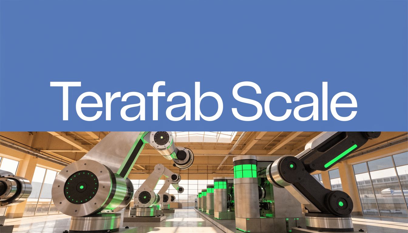
This infographic gives you a sense of the colossal physical footprint this investment is creating.

As you can see, the planned 100 million square foot facility makes even Giga Texas look small. Building this big isn't just for show; it’s a calculated play to lock in a strategic advantage in the AI arms race for years to come.
Comparing the AI Investment Landscape
So, how does Terafab’s budget stack up against the established giants of the semiconductor world? The short answer: it puts them in the same league right out of the gate.
| Company/Project | Capital Expenditure (Approx. Annual) | Context |
|---|---|---|
| Terafab (Prototype) | $20 – $25 Billion | Initial one-time cost for the first facility. |
| TSMC | ~$30 Billion | Annual budget for the world's largest chip foundry. |
| Intel | ~$25 Billion | Annual budget for a leading U.S. chip manufacturer. |
| Samsung (Semiconductor) | ~$35 Billion | Annual budget for their chip division. |
This isn't a side project. Putting this much capital on the table shows that Tesla, SpaceX, and xAI are done being just customers. They’re making a direct financial challenge to the industry's biggest players.
How Terafab Compares to Other Global Megaprojects
Trying to compare Terafab to a regular factory is like comparing a cruise ship to a rowboat. The scale is so different that you need a whole new frame of reference. This project doesn't just sit alongside other tech facilities; it belongs in the same conversation as global megaprojects—the kind of massive undertakings that define an era.
Let's start with the price tag. The $25 billion cost is just for the prototype. That initial investment alone puts it in a very exclusive club.
Real-world example: The expansion of King Khalid International Airport in Saudi Arabia is a multi-year project costing an estimated $20-30 billion. Terafab's prototype costs the same as transforming an entire international air hub. Similarly, the Three Gorges Dam in China, one of the largest power stations in the world, cost around $30 billion.
Putting Scale into Context
But the money is only half the story. The sheer physical size is where things get truly mind-boggling. The plan for the full-scale facility calls for 100 million square feet of space. This isn't a factory; it's a small city dedicated to manufacturing.

When you stack the numbers against other famous large-scale projects, you can really see what makes Terafab unique.
Terafab Scale vs. Global Megaprojects
The table below gives you a sense of where Terafab fits in the modern world of construction marvels.
| Project | Estimated Cost (USD) | Notable Scale Metric |
|---|---|---|
| Terafab (Prototype) | $25 Billion | 2 Million sq. ft. ground footprint (multi-story) |
| International Space Station | $150 Billion+ (lifetime) | Orbits Earth every 90 minutes |
| Giga Texas | ~$1-2 Billion (initial build) | 10 Million sq. ft. of factory space |
| King Khalid International Airport | ~$20-30 Billion (expansion) | 81 sq. mi. total area |
| Three Gorges Dam | ~$30 Billion | 22,500 MW power capacity |
What this shows is that Terafab is a rare beast. While something like the International Space Station has a much higher lifetime cost, Terafab's upfront capital for a single facility is staggering. It blends immense cost, a massive physical footprint, and next-generation technological complexity all in one package.
This isn’t just about building something big. It’s about creating a purpose-built ecosystem for the most advanced manufacturing on the planet. The project’s size reflects the immense infrastructure needed to power the future of AI—what some experts now see as a new form of digital labor. You can read more on how AI is changing the workforce in our deep dive into the future of AI.
Understanding the Strategic Scope of Vertical Integration
To get a real sense of the Terafab project, you have to look past the price tag and the sheer size of the building. The true scale is in its ambition. This isn't just another chip factory. It’s a bold attempt to create a self-contained world for semiconductors.
Think of it as bringing every single step of making a chip, from a rough idea to a finished AI processor, under one massive roof. This move is designed to completely sidestep the tangled and often fragile global supply chain that the entire semiconductor industry currently relies on.
The Stages of In-House Production
So what does "vertical integration" actually look like here? It means Musk's companies are aiming to control the entire life of a chip, from birth to deployment.
- Chip Design: This is where it starts. They’ll be creating the blueprints for custom processors built specifically for the neural networks running in Tesla cars and at xAI.
- Lithography & Fabrication: This is the heart of the operation—the incredibly complex and expensive process of actually etching circuits onto silicon wafers.
- Memory Production: They even plan to make their own memory, a critical component usually bought from outside suppliers like Micron.
- Advanced Packaging: The final step involves bundling the chip into a working package. This used to be an afterthought, but now it's a huge factor in a chip's final performance.
This "foundry under one roof" approach is a direct answer to the supply chain nightmares that have been holding back the tech world for years. If you want to understand the risks of relying on outside players, our guide on the benefits and drawbacks of cloud computing breaks down a similar dynamic.

Why Vertical Integration Is the Ultimate Goal
By taking control of every step, companies like Tesla, SpaceX, and xAI get a massive leg up on competitors who have to wait in line at third-party foundries like TSMC or Samsung.
The ultimate purpose of this integration is to achieve 'supply chain independence.' This means accelerating innovation, guaranteeing chip supply, and de-risking development from geopolitical tensions or market shortages.
Real-world example: During the 2021-2023 chip shortages, automakers lost an estimated $210 billion in revenue because they couldn't get enough semiconductors. Ford, for instance, had thousands of nearly-finished trucks parked in lots, waiting for a handful of chips. By building Terafab, Musk is essentially building a fortress to prevent that from ever happening to his companies again.
It’s a strategy that turns one of the industry's biggest weaknesses—depending on others for critical parts—into a powerful competitive advantage. The ability to design, build, and deploy custom hardware at this scale isn't something you can just buy on the open market. It’s a long-term play to own the engine that will power the future of AI.
What Terafab Means for the Tech Industry and Investors
When a project has a price tag this big, you know it’s going to make waves. For the semiconductor industry, Terafab isn't just another competitor—it's a direct shot at the long-standing foundry model dominated by giants like TSMC and Samsung.
This move signals a massive strategic pivot. One of the world's biggest buyers of AI chips is flipping the script to become a major producer. This forces the rest of the industry to imagine a world where their largest customers decide to just build their own supply chains, completely upending the market.
Implications for the Tech Sector
The ripple effects extend far beyond just chip manufacturing, touching everything from robotics to the need to explore AI automation solutions. By bringing chip production in-house, Musk's companies get a serious edge. This kind of vertical integration could easily inspire other tech titans to follow suit, leading to a much more fragmented—and fiercely competitive—semiconductor landscape.
- Shaking Up the Old Guard: Terafab pressures established foundries by taking a huge customer off the table and introducing a new, highly specialized competitor.
- Putting Innovation on Fast-Forward: With a dedicated foundry, Tesla and xAI can design chips perfectly tailored to their software. This could dramatically speed up breakthroughs in self-driving technology and AI research.
- A New Playbook: If Terafab works, you can bet other "hyperscalers" like Google, Amazon, and Microsoft will start thinking a lot harder about taking control of their own chip production.
A High-Stakes Game for Investors
For investors, this is the definition of a high-risk, high-reward play. The $20-25 billion needed just for the prototype is a monumental bet. And there’s no guarantee of success—chip manufacturing is notoriously complex and unforgiving.
For investors, Terafab represents both a monumental risk and a potential game-changing opportunity, fundamentally reshaping the strategic outlook for Tesla and its sister companies.
But the potential payoff is just as massive. If Terafab delivers, it could give Musk’s empire an almost unbeatable long-term advantage in the race for Artificial General Intelligence (AGI). When you control the supply of compute, you control the fuel for every future AI innovation.
That’s why understanding the different generative AI business applications is so vital to seeing the project's real value. For anyone invested in Tesla or the wider AI ecosystem, Terafab isn't just another factory. It's a critical piece of a long-term strategic puzzle that could redefine the entire industry.
Frequently Asked Questions (FAQ) about the Terafab Project
A project of this scale generates many questions. Here are clear, concise answers to the top 10 most frequently asked questions about Terafab.
1. Where Is Terafab Being Built?
The first prototype facility is under construction at the Giga Texas North Campus in Austin, Texas. However, the ultimate 100-million-square-foot facility is too large for the current site and will require a new, yet-to-be-announced location.
2. What's the Main Goal of the Project?
The primary goal is to achieve 'supply chain independence' for AI chips. By bringing the entire semiconductor manufacturing process in-house, Elon Musk's companies (Tesla, SpaceX, xAI) aim to secure the massive supply of custom hardware needed for their ambitious goals in autonomous driving, space exploration, and advanced AI.
3. Which Companies Are Behind Terafab?
Terafab is a strategic joint venture between Tesla, SpaceX, and xAI. This collaboration pools resources to address a shared, critical need for vast amounts of specialized AI computing power.
4. How Much Will Terafab Cost?
The initial prototype facility alone is estimated to cost between $20 and $25 billion. The total cost for the full-scale project will be significantly higher, likely placing it among the most expensive private industrial projects in history.
5. What Kind of Chips Will It Make?
Terafab will specialize in producing advanced, custom-designed AI accelerator chips. These are not general-purpose CPUs but highly specialized processors optimized for the massive parallel computations required for AI training (developing models) and inference (running models in real-world applications).
6. How Does This Affect Competitors Like TSMC and NVIDIA?
It presents a dual challenge. First, it removes a massive customer from the market, as Tesla and xAI will no longer need to buy as many chips from NVIDIA or use foundries like TSMC. Second, it introduces a new, well-funded competitor into the high-end chip manufacturing space, potentially inspiring other large tech companies to do the same.
7. What Is the Timeline for the Terafab Project?
The project was officially announced in March 2026 with an "aggressive" timeline. While specific completion dates are not public, constructing a leading-edge semiconductor fab of this complexity typically takes 3-5 years. The prototype could be operational in some capacity by the late 2020s, with the full-scale vision being a longer-term goal.
8. Why Is Vertical Integration So Important for This Project?
Vertical integration gives complete control over the chip development lifecycle. This allows for:
- Faster Innovation: Tightly coupling chip design with software needs.
- Guaranteed Supply: Eliminating dependence on external suppliers and geopolitical risks.
- Customization: Creating chips perfectly optimized for specific tasks, like Tesla's self-driving software.
- Cost Control: Potentially lowering per-unit costs at extreme scale.
9. Is a $25 Billion Investment a Huge Risk?
Yes, it is an enormous financial and technical risk. Semiconductor manufacturing is one of the most complex and capital-intensive industries in the world, with razor-thin margins for error. However, from the project's perspective, the strategic risk of not securing a dedicated supply of AI chips is considered even greater.
10. Will Terafab Sell Chips to Other Companies?
Initially, no. The entire output of Terafab is planned for internal consumption by Tesla, SpaceX, and xAI to meet their enormous demand for AI compute. While Musk has not entirely ruled out acting as a foundry for other companies in the distant future, the primary and sole focus for the foreseeable future is to serve its parent companies.
For more insights on tech, finance, and innovation, stay updated with Everyday Next. Explore our latest articles at https://everydaynext.com.
Related Posts
Previous Post
Next Post