
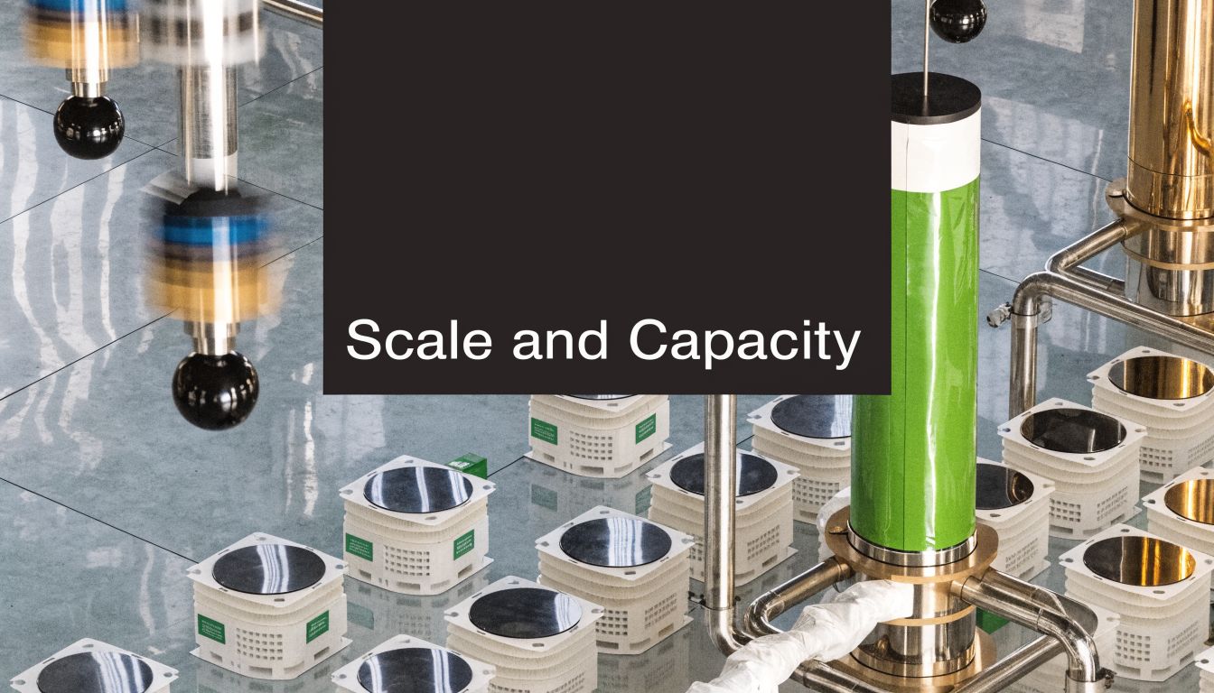
TeraFab Size, Capacity and Power Needs: What We Know
Last fact-checked: October 13, 2026. TeraFab’s official vision shows more than 100 million square feet of manufacturing space with a long-term goal of producing chips representing one terawatt of annual compute capacity. Those are announced targets, not operating results. The most useful way to understand TeraFab’s scale is to separate the Austin research fab, the first Grimes County phase and the ultimate multi-phase vision.
Key distinction: TeraFab’s “one terawatt per year” claim describes the planned compute capacity of chips produced annually. It is not a statement that the factory currently consumes or generates one terawatt of electricity.
TeraFab size and capacity claims
| Metric | Current public figure | How to interpret it |
|---|---|---|
| Full-scale footprint | 100 million square feet | Official long-term concept for the Grimes County complex, not completed floor area |
| Annual compute output | 1 TW per year | Company target for the chips produced, not current production or factory electricity use |
| Energy vision | More than 1 TW of solar power | Official presentation of the broader orbital-compute ambition, not an approved utility load for the factory |
| Initial announced investment | $16.8 billion | First-phase commitment announced by SpaceX and Tesla in August 2026 |
| Potential investment | Up to $119 billion across later phases | Maximum expansion figure reported from project filings; not committed spending |
| Employment | At least 3,000 jobs | Company projection for the full-scale site |
| Research-fab capacity | A few thousand wafers per month | Earlier description of the smaller Tesla research facility near Giga Texas |
| On-site electricity | On-site power plant or plants plus battery storage are expected | The fully executed county agreement does not disclose a 2-gigawatt capacity |
| 100–200 billion chips per year | Widely repeated estimate, not a current verified production commitment | Musk’s primary presentation described 100–200 gigawatts of terrestrial compute output, which is a different measure |
Three different scales are often confused
1. Research fab
Tesla’s research fab at the North Campus of Giga Texas is intended to test manufacturing ideas and processes. Elon Musk described it as a facility capable of producing a few thousand wafers per month. That scale can support learning, qualification and small-batch work. It is not the million-unit industrial system implied by the long-term presentation.
2. Initial Grimes County phase
SpaceX and Tesla announced an initial $16.8 billion investment in August 2026. This phase is associated with a site in Grimes County near the Gibbons Creek Reservoir. It is expected to manufacture, package and test advanced logic and memory chips. The companies have not published enough engineering detail to calculate a dependable wafer-start figure or completion date.
3. Full TeraFab vision
The official project material illustrates a 100-million-square-foot complex and one terawatt of compute output per year. Reaching that vision would require multiple construction phases, large utility systems, extensive equipment installation, process qualification, thousands of skilled workers and a sustained ramp in manufacturing yield.
How large is 100 million square feet?
One hundred million square feet equals roughly 9.3 million square metres or 3.6 square miles of floor area. It also converts mathematically to about 2,296 acres, but that does not establish a 2,300-acre land parcel. A multi-building or multi-level campus can have floor area that differs substantially from its land footprint. The official presentation compares the plan with Tesla’s roughly 10-million-square-foot Texas Gigafactory, implying about ten times the illustrative floor area.
If the full plan is completed, it would rank among the largest manufacturing complexes ever proposed. Calling it definitively “the largest physical manufacturing facility on Earth” is premature because the build is phased and reports do not consistently distinguish one building from a wider campus. Comparisons with the Pentagon are also unreliable when one source uses total floor area and another uses building footprint.
Floor area alone does not determine semiconductor output. A large campus may contain cleanrooms, chemical and gas systems, water treatment, power distribution, warehouses, packaging lines, offices, testing areas and buffer space. Only part of the footprint directly processes wafers.
Useful capacity measures include:
- wafer starts per month;
- the process nodes being qualified;
- cycle time through the fab;
- yield, or the percentage of usable dies;
- advanced-packaging throughput;
- memory availability;
- tool utilization and downtime; and
- the number of chips that meet reliability requirements.
Until those figures are disclosed, square-foot comparisons should be treated as a description of ambition rather than proof of output.
Compute output versus electricity use
The word “terawatt” creates confusion because watts usually describe power. TeraFab’s one-terawatt-per-year headline is a company framing for the compute capacity embodied in the chips produced annually. It does not tell readers the factory’s electrical demand.
Semiconductor plants nevertheless use substantial electricity. Major loads include lithography equipment, vacuum pumps, cleanroom air handling, cooling, process tools and water systems. The fully executed Grimes County tax-abatement agreement says the project expects to build on-site natural-gas-fired power generation and battery storage rather than rely on the grid, but it does not disclose the generating capacity. The widely repeated two-gigawatt figure therefore should not be presented as confirmed. The official TeraFab presentation separately says the wider vision needs more than one terawatt of solar power; that refers to the scale of the planned AI-compute system, including space-based infrastructure, not the approved electrical load or output of the Texas fab.
Does TeraFab plan to make 100–200 billion chips a year?
That figure appears in secondary coverage, but it is not a current verified production commitment. In Musk’s March 2026 presentation, the 100–200 figure referred to gigawatts of terrestrial compute output per year, with the balance of a roughly one-terawatt goal intended for space-based computing. Gigawatts of compute and a count of packaged chips are not interchangeable. Without a disclosed product mix, die size, wafer starts, yield and packaging throughput, a defensible annual chip count cannot be calculated.
Water requirements
Chip manufacturing uses ultra-pure water to clean wafers between process steps. Reuters reported that the Grimes County site plans to use water from the nearby Gibbons Creek Reservoir rather than local groundwater.
The meaningful questions are how much water each phase will withdraw, how much can be recycled, how wastewater will be treated, and which permits will govern operations. A reservoir location reduces one concern but does not replace a full water-impact analysis.
What could limit the build-out?
Equipment availability
Leading-edge fabs depend on a concentrated set of suppliers. Lithography, deposition, etch, metrology and packaging tools often have long lead times. A large building without qualified equipment does not create chip capacity.
Process maturity and yield
Musk has said TeraFab plans to use Intel’s 14A process. That technology was still developing when announced. Stable yield matters more than a node label because low yield makes otherwise impressive wafer capacity uneconomic.
Power and construction
The site needs dependable power, substations, backup systems, cleanroom construction and specialized contractors. Each expansion phase has to be synchronized with utilities and equipment delivery.
Talent
Process integration, equipment engineering, materials science, yield analysis and advanced packaging require experienced teams. Recruiting 3,000 workers is different from assembling 3,000 people with the required semiconductor experience.
How TeraFab compares with an established foundry
TSMC’s advantage is not merely floor space. It has decades of manufacturing data, customer qualification, supplier relationships and yield learning across many products. TeraFab’s proposed advantage is tighter integration with a smaller number of internal product roadmaps.
That means TeraFab does not need to replace TSMC globally to become strategically useful. Even a smaller, reliable output could provide dedicated capacity and faster design feedback. See our TeraFab, TSMC and Nvidia comparison.
Milestones that would prove real capacity
- Public permits and completed utility agreements.
- Finished cleanroom space and installed production tools.
- Intel 14A or another process qualified at the site.
- Named products completing test wafers.
- Published wafer starts and yield progress.
- Qualified packaging and memory integration.
- Shipment of production chips into Tesla or SpaceX systems.
Announcements about investment and footprint are early indicators. Tool installation, yield and product qualification are the indicators that turn a construction project into a working fab.
Frequently asked questions
Is TeraFab really 100 million square feet?
That is the official long-term target. It should not be described as completed or operating space.
Will TeraFab produce one million wafers per month?
Some coverage has repeated large wafer targets, but current official material emphasizes square footage and compute output. A dependable wafer-start target needs direct company documentation and should include the relevant phase and date.
Where is the factory?
The research facility is near Giga Texas. The announced full-scale complex is in Grimes County, Texas, near the Gibbons Creek Reservoir.
When will it be finished?
No single verified date exists for the full vision. The project is phased, and a research facility, initial production phase and complete build-out should not be assigned the same completion date.
Will TeraFab have a two-gigawatt power plant?
No public primary document reviewed for this update confirms a two-gigawatt capacity. The executed county agreement does support plans for on-site natural-gas generation and battery storage, but it does not state the system’s size.
Will TeraFab make 100–200 billion chips annually?
That is not a verified current commitment. The primary presentation described 100–200 gigawatts of annual terrestrial compute output—not 100–200 billion individual chips—and did not disclose the product and manufacturing data needed to convert that target into a chip count.
Sources
- Official TeraFab scale and product presentation
- SpaceX: August 6, 2026 TeraFab announcement
- Reuters: Grimes County investment, site and employment
- Reuters: research fab and Intel 14A plan
- Transcript of Musk’s March 2026 TeraFab presentation
- Grimes County: fully executed SpaceX tax-abatement agreement
Start with the complete TeraFab explainer, or follow current permits and construction in our TeraFab Texas status tracker.
Related Posts
Previous Post
Next Post








Pingback: TeraFab Texas: Location, Timeline and Latest Status