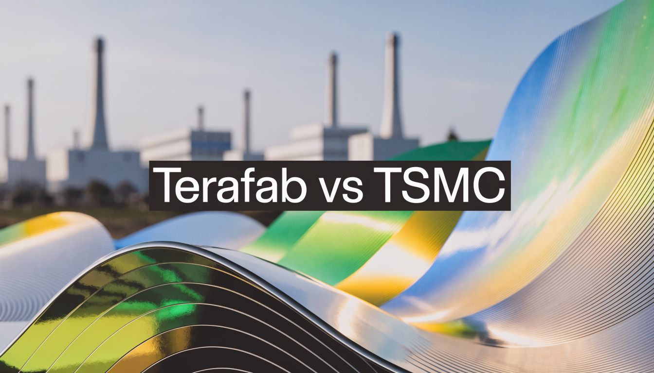
Terafab Vs TSMC Comparison Explained: 2026 Analysis
Terafab is aiming at a scale that would force investors to stop thinking about chip fabs as incremental infrastructure. Its target is 1 million wafers per month by 2030, versus approximately 140,000 wafers monthly at TSMC's current most advanced 2nm production, according to AInvest's report on Terafab's capacity ambitions. If that target is even partially realized, this stops being a supplier story and becomes a power shift across AI, autonomy, robotics, and aerospace.
That's why a terafab vs tsmc comparison explained properly can't be reduced to node names or factory size. The primary conflict is between two manufacturing ideologies. TSMC built its advantage through specialization, customer trust, and a global supplier web. Terafab is the opposite bet. One roof, tighter control, faster iteration, and far higher execution risk.
For smart investors and tech operators, the useful question isn't “Who wins?” It's “Which model matters more for the next decade of AI hardware: proven yield discipline or vertically integrated speed?”
Table of Contents
- The Coming Collision in Semiconductor Manufacturing
- A Tale of Two Titans TSMC and Terafab
- Comparing Process Nodes and Technology Leadership
- Manufacturing Capacity and Supply Chain Strategy
- A Clash of Business Models Vertical Integration vs The Ecosystem
- Analyzing Strategic Strengths and Critical Risks
- The Bottom Line for Investors and Technologists
- Frequently Asked Questions About Terafab and TSMC
The Coming Collision in Semiconductor Manufacturing
The semiconductor industry rarely produces a clean philosophical showdown. This one does. TSMC represents the most refined version of the foundry model ever built. Terafab represents a challenge from outside that system, backed by companies that increasingly see chip supply as too important to outsource indefinitely.

The stakes go well beyond fabs. Tesla, xAI, and SpaceX want chips for self-driving systems, robots, AI clusters, and potentially space-oriented computing infrastructure. TSMC, by contrast, sits at the center of the existing global model. It manufactures for a wide range of major technology companies and has spent decades turning process discipline into strategic power.
That makes this battle relevant to anyone tracking AI infrastructure, industrial policy, or manufacturing resilience. It also intersects with wider trade and localization pressures, which readers can see in this broader look at how new trade tariffs in 2025 are changing strategy.
The real disruption isn't just more wafer capacity. It's the attempt to compress chip design, fabrication, packaging, and feedback into one industrial loop.
For investors, this matters because both outcomes are investable. If Terafab works, vertical integration becomes more credible for large AI buyers. If it struggles, TSMC's moat looks even wider because it would confirm how hard leading-edge manufacturing still is.
A Tale of Two Titans TSMC and Terafab
More than 60 percent of the world's foundry revenue flows through one company, according to industry trackers. That concentration is the starting point for any serious Terafab vs. TSMC comparison, because this contest is less about a new fab announcement than about whether the semiconductor industry's dominant operating model can be challenged.
TSMC represents the established logic of the sector. It built trust by staying focused on manufacturing, letting customers design chips while it mastered yield, process transitions, packaging, and scale. That division of labor created a powerful ecosystem effect. The more leading chip companies relied on TSMC, the more attractive TSMC became to equipment vendors, materials suppliers, and advanced packaging partners.
TSMC as the reference standard
TSMC's advantage is industrial, not rhetorical. Years of execution have made it the default manufacturing partner for companies that need cutting-edge output and predictable delivery. Investors should view that as a structural asset. In semiconductors, consistency in yield and ramp timing usually matters more than headline ambitions.
Its current posture reflects confidence in demand and in its own model. TSMC is still expanding geographically and technologically, while preserving the customer neutrality that made the foundry model work in the first place. That matters because a neutral manufacturer can aggregate demand across smartphones, AI accelerators, automotive chips, and data center processors. A captive fab cannot.
The result is a business with unusually strong strategic gravity. Customers may want supply diversification, but few can afford to move meaningful advanced-node volume to an unproven alternative unless the economics or the supply risk become compelling.
Terafab as a strategic break from outsourcing
Terafab starts from a different premise. For Tesla, xAI, and SpaceX, chip supply is no longer a procurement issue alone. It affects product roadmaps, AI training schedules, vehicle compute platforms, and the speed at which hardware feedback can be folded back into design.
That makes Terafab a high-risk attempt to compress more of the semiconductor loop inside one corporate orbit. The logic resembles the broader push toward ownership of scarce AI infrastructure that is reshaping capital allocation across the sector, as seen in the strongest generative AI investment opportunities tied to compute demand.
TSMC monetizes manufacturing excellence across a broad customer base. Terafab aims to use manufacturing control to improve the economics and timing of a narrower set of internal priorities.
That difference sounds subtle. It is not.
TSMC wins by serving many chip designers well enough that none of them need to build a rival ecosystem from scratch. Terafab would win on a different metric. It only needs to reduce dependence for its owners, shorten iteration cycles, or secure capacity during periods when outside foundries are constrained.
Investor lens: Terafab does not need to match TSMC's scale to affect the market. If it improves supply assurance or product cadence for Musk-linked companies, it could still influence pricing power, customer bargaining dynamics, and the long-term case for vertical integration in AI hardware.
Comparing Process Nodes and Technology Leadership
ASML's latest EUV tools can process hundreds of wafers per hour, but that throughput figure matters only if a fab can convert it into stable yields over months of production. That is the real test in any terafab vs tsmc comparison explained for investors.

Why node names still matter
Node labels still carry economic meaning, even if they no longer map cleanly to a single physical dimension. For buyers of AI accelerators and automotive compute, a better process can improve transistor density, power efficiency, thermals, and total system performance. Those gains shape server economics, training cluster design, and vehicle compute envelopes.
TSMC's lead comes from industrial execution, not branding. Years of process tuning, supplier coordination, defect reduction, and customer tape-out experience have turned advanced-node manufacturing into a repeatable operating discipline. That ecosystem-driven model is difficult to replicate because it compounds know-how across many customers and many product cycles.
Terafab is attempting something different. Its upside does not come from merely matching a node label. It comes from pairing advanced manufacturing with a tighter internal design-to-production loop for AI and automotive chips. That could matter if the companies tied to its output value speed, capacity assurance, and design feedback more than broad external customer support. Investors tracking the compute buildout behind that thesis can also review these generative AI investment opportunities tied to infrastructure demand.
Tooling determines whether plans become shipments
The equipment stack sets the floor for credibility. According to Tom's Hardware coverage of Samsung's Texas fab and Musk's comments, Samsung's Taylor facility uses Twinscan NXE:3800E EUV systems rated at 220 wafers per hour. The same report frames that toolset as more advanced than the older equipment used in TSMC's Fab 21 Phase 1.
That matters because advanced manufacturing is constrained by access to very specific tools, then by the ability to integrate, calibrate, and maintain them at production scale. Terafab therefore faces a two-part challenge. It must secure top-tier equipment in a market with long lead times and geopolitical sensitivity. It must then prove that a new organization can turn those tools into commercially reliable output.
The comparison is clearer in operating terms:
| Technology issue | TSMC position | Terafab challenge |
|---|---|---|
| Advanced-node execution | Established manufacturing discipline | Must prove it can ramp from scratch |
| EUV tooling integration | Known operating experience | Must secure and operationalize top-tier equipment |
| Yield learning | Built on years of process history | Faces a steep learning curve |
| Product fit | General foundry support | Can optimize for internal AI and automotive use cases |
This short video highlights the manufacturing and tooling race behind advanced-node competition, which is relevant because tool quality alone does not guarantee repeatable output.
Why Repeatability Matters More Than Node Names
Matching a node label does not mean matching manufacturing capability. In practice, leadership at the leading edge is defined by repeatability, yield consistency, and the ability to hold process control across high volumes.
TSMC starts ahead because it has already solved those problems multiple times. Terafab represents a higher-risk, vertically integrated bet. If it works, it could compress iteration cycles for internal AI programs and change how investors value supply control. If it stumbles, the gap between ambitious process targets and profitable production will remain wide.
Manufacturing Capacity and Supply Chain Strategy
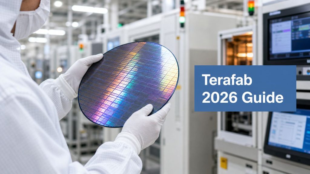
1 million wafers per month by 2030 is the figure that turns Terafab from an ambitious fab project into a direct challenge to the dominant logic of advanced semiconductor manufacturing.

Early comparison snapshot
Capacity matters here, but the larger issue is how each company intends to create reliable output at scale.
| Company | Manufacturing philosophy | Strategic emphasis | Main trade-off |
|---|---|---|---|
| Terafab | Vertical integration | Speed, control, internal supply | High execution risk |
| TSMC | Ecosystem foundry | Reliability, specialization, customer breadth | More logistical latency |
Scale is a supply chain argument
AInvest's report on Terafab's planned output and investment says the project targets 1 million wafers per month by 2030, up from 100,000 wafers per month between now and 2027, with projected annual output of 100 to 200 billion chips. The same report puts the initial investment at $20 billion to $25 billion, with another $10 billion to $15 billion potentially required.
If those targets are taken at face value, Terafab is not trying to become a smaller version of TSMC. It is trying to replace a distributed supplier web with a tightly controlled industrial stack built around the compute needs of affiliated businesses such as Tesla, SpaceX, and xAI. That could shorten design-to-production cycles and protect internal customers from external foundry bottlenecks. It also concentrates more risk into one site, one operating model, and one management team.
TSMC uses the opposite logic. It spreads capacity across multiple geographies, process generations, and customer programs. That structure can be slower to reconfigure, but it reduces the odds that a single bottleneck in power, packaging, labor, or local infrastructure disrupts the entire system. The wider manufacturing field is already moving toward higher automation intensity, as seen in China's surge in industrial robot production and what it signals for factory automation.
One question matters more than the headline wafer number. Can every supporting layer scale at the same pace?
Capacity table
| Metric | Terafab (Target) | TSMC (Current/Planned) |
|---|---|---|
| Wafer output ambition | 1 million wafers per month by 2030 | As noted earlier, TSMC scales through a distributed leading-edge network rather than a single-site concentration |
| Near-term ramp | 100,000 wafers per month between now and 2027 | Capacity additions continue across Taiwan, Arizona, and Japan, as noted earlier |
| Annual chip output | 100 to 200 billion chips | Output is diversified across a broad customer and fab base |
| Strategic structure | Single integrated site | Multi-site foundry network |
| Capital commitment | $20 billion to $25 billion initially, with possible $10 billion to $15 billion more | TSMC continues to fund expansion through its established multi-year capital spending program, as noted earlier |
For investors, the practical test is operational synchronization. Wafer starts alone do not create economic value. Power availability, EUV tool uptime, advanced packaging throughput, materials supply, and yield stability have to expand together. A vertically integrated system can move faster when it works. It can also fail in a more correlated way.
That is the core divide. TSMC distributes complexity across an ecosystem. Terafab is betting that collapsing complexity into one loop will produce a strategic advantage large enough to justify the execution risk.
A Clash of Business Models Vertical Integration vs The Ecosystem
The cleanest way to understand this rivalry is to ignore the branding and look at factory logic. Terafab and TSMC are trying to solve different problems.

Terafab's recursive loop
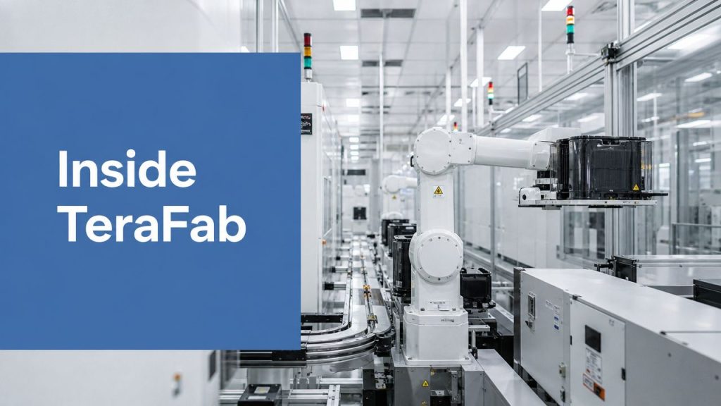
Terafab's core idea is that chip development slows down when design, masks, fabrication, packaging, memory, and testing are split across organizations and locations. According to this YouTube analysis of Terafab's vertically integrated model, Terafab aims to put every production stage under one roof in Austin, with the goal that a Tesla engineer could design, fabricate, test, debug, and iterate a chip within a single day. The same analysis contrasts that with TSMC's orchestration of around 3,000 specialized global suppliers.
That matters most for custom AI accelerators. If your product roadmap changes quickly, waiting on external handoffs becomes expensive in ways that don't show up clearly on a standard manufacturing spreadsheet.
Terafab is effectively saying that for internal products like AI5 chips, autonomy silicon, robotics processors, and space-related compute, speed of iteration may be more valuable than foundry neutrality.
TSMC's ecosystem machine
TSMC's model is less dramatic, but it's proven. It coordinates a huge network of specialist suppliers and manufacturing steps because that system has historically produced the highest reliability at the leading edge. Customers don't go to TSMC because it is simple. They go because the complexity has already been mastered.
A direct side-by-side helps:
- Terafab optimizes for control. It wants fewer handoffs and faster feedback.
- TSMC optimizes for dependability. It turns supplier coordination into manufacturable output at scale.
- Terafab is internally biased. It can favor the needs of Tesla, xAI, and SpaceX.
- TSMC is externally oriented. It serves many customers with a repeatable process discipline.
If Terafab succeeds, it won't prove TSMC's model is obsolete. It will prove that some AI-heavy companies value design speed enough to absorb fab risk themselves.
This is why the business model clash matters more than the headline rivalry. TSMC built the industry standard for horizontal specialization. Terafab is testing whether the AI era rewards a more vertically integrated stack.
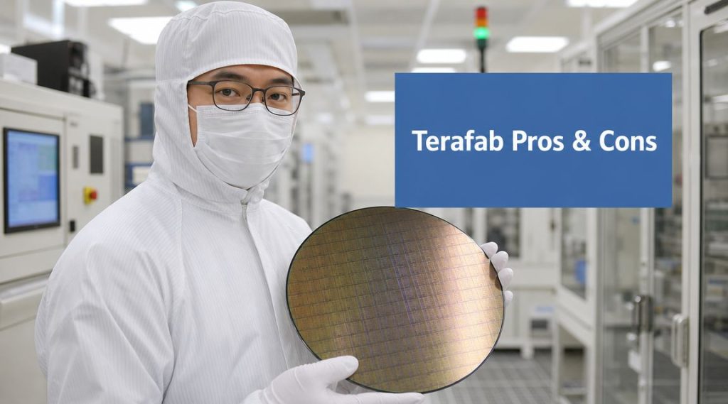
Analyzing Strategic Strengths and Critical Risks
Advanced-node manufacturing failures rarely show up as a single missed milestone. They show up as compounding delays, weak yields, expensive rework, and product roadmaps that slip out of sync with the markets they were built to serve.
That framing matters here because Terafab and TSMC are playing different games. Terafab is pursuing a high-risk operating model built around internal speed, tighter design-manufacturing feedback, and greater control over strategic silicon. TSMC is defending a system built on process maturity, supplier depth, and repeatability across many customers. For investors, the question is less about who has the better story and more about which manufacturing philosophy produces better economic results under pressure.
Where Terafab could become a real threat
Terafab's primary upside is iteration speed, which offers more than supply independence. If Tesla can shorten the path from design change to tested silicon, it could improve chip development for AI training, autonomy, robotics, and other programs where requirements shift quickly.
That advantage is real only if the fab can convert speed into usable output.
Public reporting and industry commentary around Terafab consistently point to the same tension. A vertically integrated fab may reduce handoff friction and shorten internal cycle times, but early-stage semiconductor manufacturing usually suffers from yield instability, equipment tuning issues, and slower-than-expected ramp curves. Those problems matter more than slide-deck timelines because bad wafers distort engineering feedback and inflate cost per working chip.
The capital burden is just as important. Terafab is not testing a small process improvement. It is testing whether one company can absorb the execution risk that the broader foundry ecosystem has spent decades distributing across specialized partners. If that works, the reward is strategic control over a core AI bottleneck. If it fails, the penalty is years of capex tied up in an asset that underperforms precisely when demand is strongest.
Why TSMC still holds the stronger strategic position
TSMC's edge comes from accumulated manufacturing discipline. Process history, customer qualification experience, supplier coordination, and defect reduction methods create an advantage that is difficult to compress into a short period, even with large capital spending.
That matters because advanced logic is not won by headline node claims alone. It is won by turning process technology into predictable volume output, with enough consistency that customers can plan product launches, power budgets, and gross margins around it.
Its weaker point is strategic flexibility. TSMC is optimized for a broad customer base and a standardized operating model. Terafab, if it works, would be designed for the priorities of one tightly linked corporate group. That can matter in AI, where product requirements can change faster than traditional foundry planning cycles.
| Category | Terafab | TSMC |
|---|---|---|
| Main strategic upside | Faster internal learning cycles and tighter product-fab coordination | Proven execution at leading-edge scale |
| Main operational risk | Ramp failure, weak early yields, and capex overhang | Lower flexibility for highly proprietary, fast-changing internal programs |
| Supply chain posture | Concentrates more activity inside one corporate stack | Spreads execution across a mature specialist ecosystem |
| Investor question | Can speed offset manufacturing inexperience? | Can the ecosystem model stay dominant as AI companies seek more control? |
TSMC also carries concentrated geopolitical exposure because so much advanced manufacturing remains linked to Taiwan. That issue sits inside a broader pattern of export concentration and industrial dependence, which is outlined in this review of the largest exporters of 2023 and their impact on the global economy.
In semiconductors, reliability is a pricing power asset. Customers will often pay more to avoid uncertainty in yield, timing, and volume.
The real risk test
Terafab has to prove two things in parallel. It must show that vertical integration produces faster, commercially useful design learning. It must also show that manufacturing quality improves quickly enough to keep those faster cycles credible.
If only the first happens, Terafab remains an internal strategic tool with limited external significance. If only the second happens, it looks more like an expensive domestic capacity project than a new model for AI-era semiconductor production.
TSMC's bar is lower. It does not need to copy Terafab's structure to remain dominant. It needs to preserve the industry's most trusted path to advanced-node volume while watching for a narrow but important shift in customer behavior: whether the biggest AI buyers decide that control over iteration is worth taking on fab risk themselves.
The Bottom Line for Investors and Technologists
The most important conclusion is that Terafab and TSMC are not pure substitutes. They can coexist, and in the near term they likely will.
What Tesla investors should focus on
According to Wikipedia's summary of Terafab-related sourcing and leverage claims, Musk continues placing large orders with TSMC, using Terafab as a “bargaining chip” to secure better terms. The same entry says Tesla's 2025 TSMC orders are over $10B, up 50% year over year, and that Tesla secured a 15% volume discount.
That turns Terafab into a strategic option, not just a manufacturing plan. Even before it proves full-scale output, it can shape negotiations, diversify sourcing logic, and reduce the chance that Tesla is trapped by a single external supplier.
For Tesla investors, the right lens isn't “Terafab replaces TSMC.” It's this:
- Base case: TSMC remains the core advanced manufacturing partner.
- Strategic upside: Terafab improves bargaining power and internal optionality.
- Execution risk: If the fab ramp struggles, capex and timelines become the problem.
Anyone approaching this from a public-markets angle may also want a broader framework for chip exposure through listed names, such as this beginner-oriented guide on how to invest in Nvidia.
What chip industry professionals should watch
For technologists, Terafab matters because it tests whether a hyperscaler-style manufacturing model can extend into leading-edge semiconductor production. If it works, more large compute buyers may pursue tighter integration across design, packaging, and fab strategy. If it fails, the foundry model looks even more durable.
A few concrete watchpoints matter more than broad narratives:
- Tooling visibility. Advanced EUV procurement and installation are stronger signals than presentation slides.
- Talent concentration. Hiring from Taiwan and other mature clusters matters because fabs scale with people before they scale with wafers.
- Packaging and test integration. A fast fab loop breaks if backend processes remain slow.
- Customer mix. The more Terafab serves internal platforms first, the easier it is to justify specialized design choices.
For investors, Terafab is best viewed as a hedge with upside. For technologists, it's a live experiment in whether AI demand can justify a new manufacturing architecture.
The bottom line is straightforward. TSMC still owns the proof. Terafab owns the challenge.
Frequently Asked Questions About Terafab and TSMC
These questions sound simple, but the answers matter because Terafab versus TSMC is not just a specs comparison. It is a contest between a concentrated, vertically integrated manufacturing model and a foundry system built on scale, customer breadth, and decades of process learning.
| Question | Answer |
|---|---|
| What is the simplest terafab vs tsmc comparison explained in one sentence? | TSMC is the established leader in advanced contract manufacturing, while Terafab appears to be a higher-risk attempt to build tighter in-house control over chip production for Musk-affiliated platforms. |
| Is Terafab trying to replace TSMC entirely? | Current evidence points to a narrower objective. Terafab looks more like added internal capacity and a strategic hedge than a full substitute for the global foundry network Tesla and related companies still depend on. |
| Why does vertical integration matter so much here? | It can shorten the loop between chip design, fabrication, packaging, and testing. For AI programs, that matters because product requirements shift quickly, and a company with tighter internal coordination may respond faster than one working through several external suppliers. |
| Why does TSMC remain so hard to challenge? | Because leading-edge manufacturing is built on more than capital spending. TSMC's edge comes from yield discipline, process integration, supplier coordination, and years of accumulated defect reduction across many customers and product cycles. |
| Does a newer fab automatically mean better chips? | No. Newer tools are an advantage, but they do not guarantee competitive output. Yield, process integration, engineering depth, and the speed of learning during ramp are what determine whether a new fab produces strong silicon at useful scale. |
| What is Terafab's biggest strategic advantage? | Speed is the clearest upside. If Terafab can keep design teams, manufacturing, and advanced packaging in a tighter internal loop, Tesla, xAI, or SpaceX could reduce the time between architecture changes and production feedback. |
| What is Terafab's biggest risk? | Yield remains the central risk because weak early yields can drive up cost per wafer, delay product roadmaps, and erase the advantages that vertical integration is supposed to create. |
| What is TSMC's biggest strategic vulnerability? | TSMC is optimized for serving a broad customer base, not for maximizing the iteration speed of one tightly integrated buyer. That model is powerful, but it can be less responsive to customers trying to synchronize silicon development with fast-changing internal AI roadmaps. |
| Should investors treat Terafab as a near-term revenue engine? | That would be aggressive. Until there is visible proof of production quality, yield stability, and meaningful scale, Terafab is better viewed as a strategic asset and a potential negotiating tool than as a material earnings driver. |
| What should professionals watch over the next few years? | Focus on signals that are hard to fake: advanced tool installation, experienced fab hiring, packaging and test integration, and whether Terafab stays focused on internal demand or tries to attract outside customers. Those milestones will say more than announcements about whether this model can become economically credible. |
Everyday Next publishes clear, practical analysis for readers who want signal over noise across investing, technology, and innovation. If you found this breakdown useful, explore more at Everyday Next.
Related Posts
Previous Post
Next Post