Terafab Austin Factory Explained: A 2026 Deep Dive

2 months ago212 Views

Most coverage treats TeraFab like a sci-fi headline. The more revealing number is simpler: SpaceX intends to spend $55 billion upfront and potentially as much as $119 billion in total on the Austin chip project, according to public notices reported by Manufacturing Dive. That instantly changes the frame. This isn't a side project, a lab, or a branding exercise. It's an attempt to build a private semiconductor supply chain at national-infrastructure scale.

That's why “terafab austin factory explained” isn't really a story about one factory. It's a story about whether Musk's companies can stop depending so heavily on the standard chip ecosystem, where design, fabrication, packaging, and testing are usually split across different firms and geographies. If TeraFab works, Tesla, SpaceX, and related AI efforts could shorten product cycles, lock in supply, and set their own manufacturing priorities. If it stalls, the project becomes a reminder that semiconductor manufacturing punishes ambition that outruns physics, utilities, and execution.

Table of Contents

The Grand Vision Behind TeraFab

One proposed factory complex in Austin is being discussed in the context of tens of billions of dollars in spending and an output target framed as enough computing power to support Tesla vehicles, Optimus robots, and specialized SpaceX systems. That headline is large enough to attract hype on its own. The harder question is whether the vision works as an industrial system. A project on this scale has to clear three tests at once: power availability, manufacturing competence, and strategic payoff.

A modern, wavy glass and gold-toned office building structure situated next to a tranquil pond.

The usual reading is simple. Musk wants more chips under his own control. That is true, but incomplete. TeraFab appears to be an attempt to reduce dependence on outside foundries at the exact moment AI systems, autonomous vehicles, robotics, and space hardware are all pushing for more customized silicon. For Tesla and SpaceX, the attraction is not only supply assurance. It is shorter iteration cycles, tighter secrecy, and the ability to align chip roadmaps with product roadmaps instead of waiting in line behind other customers.

That ambition has practical limits. Semiconductor fabrication is one of the most power-hungry and water-sensitive forms of manufacturing in the modern economy. Austin already sits at the center of a growing data center, EV, and advanced manufacturing cluster, so TeraFab raises a less glamorous but more useful question than the marketing slogan does. Can the local grid, water system, and supplier base support a facility meant to feed several compute-heavy businesses at once? If the answer is uncertain, then the strategic value of owning the fab could be offset by bottlenecks outside the cleanroom.

This is why the project matters beyond Musk's companies. If TeraFab can handle even part of its stated mission, it changes the balance of dependence around NVIDIA, TSMC, and Intel. NVIDIA benefits today from selling the picks and shovels of the AI boom. TSMC benefits from being the manufacturing partner that many advanced chip designers cannot replace. Intel is trying to rebuild relevance by becoming a foundry and domestic manufacturing option. A successful TeraFab would not erase those positions, but it would signal that major compute buyers are serious about pulling more of the stack in-house.

The broader pattern is already visible across top tech trends of 2025. Large technology companies are committing capital to control the layers they once outsourced, especially where supply constraints can delay product launches or cap margins. Chip manufacturing is the hardest version of that strategy because it combines software-like iteration pressure with utility-scale infrastructure demands.

A useful comparison comes from the evolution of storage devices. Storage improved when advances in materials, process control, and system design moved together. TeraFab is pursuing a similar idea in semiconductors. The factory is only one piece. The core bet is that design, fabrication, packaging, and deployment can be coordinated tightly enough to produce faster product cycles and better economics than a fragmented supplier model.

What is TeraFab really buying if the build-out happens as described?

  • Priority access to manufacturing capacity for Tesla and SpaceX programs that cannot afford long external queues
  • Faster iteration between chip design and real-world testing, which matters in AI training, autonomy, and robotics
  • More specialized silicon for workloads that general-purpose suppliers may not optimize around
  • Stronger bargaining power with incumbent partners, even if those partners remain necessary for advanced process steps

The strategic logic is sound. The execution burden is enormous. That is what makes TeraFab interesting. It is not just a moonshot in chips. It is a test of whether Austin can support a private semiconductor pipeline without running into the very infrastructure constraints that have shaped the global chip industry for decades.

Inside TeraFab A Look at the Manufacturing Technology

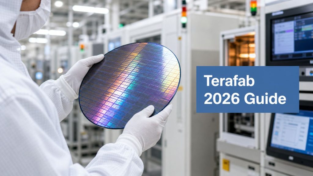
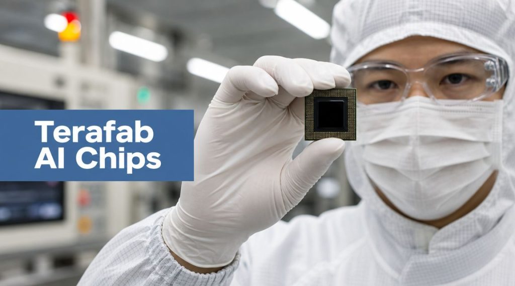
The defining feature of TeraFab isn't merely that it makes chips. It's that reports describe it as a vertically integrated complex that brings chip design, lithography, fabrication, packaging, and testing under one roof, with a pilot phase in Austin near Giga Texas and a staged ramp from small-batch production targeted for late 2026 to volume production in 2027, according to FinTech Weekly's report on TeraFab.

An infographic comparing the traditional semiconductor manufacturing model with the integrated TeraFab production process and benefits.

Why vertical integration matters

In the standard semiconductor model, a company might design a chip in one place, send the design to a foundry somewhere else, move the finished wafers to another partner for packaging, and then hand final parts to yet another company for testing. Each transfer adds time, coordination risk, and delay.

TeraFab's model aims to compress that loop. For Tesla's AI chips, especially the reported focus on faster iteration, the advantage isn't abstract. Engineers can move from design to fabricate to test to revise with fewer external handoffs.

A good analogy is a restaurant. Traditional chipmaking is like a restaurant that buys vegetables from one vendor, pasta from another, sauces from a third, and then sends finished plates to an outside kitchen for quality control. A vertically integrated restaurant grows ingredients, makes the pasta, cooks the meal, and checks quality in the same building. You don't just save transport time. You learn faster because the chef, the prep team, and the tasting team can correct mistakes together.

A real world analogy for the chip workflow

Chipmaking itself can sound opaque, so it helps to break it into plain language:

Stage What it means in practice Why co-location helps
Design Engineers define how the chip should behave Design teams can respond faster to test feedback
Lithography Patterns are placed onto wafers Process changes don't have to travel through multiple vendors
Fabrication The wafer is built layer by layer Manufacturing and design teams can troubleshoot directly
Packaging The chip is assembled into a usable form Performance tuning can continue after wafer production
Testing Engineers verify reliability and output Failures can feed back into redesign quickly

That integrated loop matters more in AI hardware than in slower product categories. Performance depends on many small design choices, and those choices often need repeated refinement. Readers interested in how physical hardware evolves over time might also appreciate this piece on the evolution of storage devices, which shows how materials science and manufacturing architecture shape performance, not just software.

Practical rule: In advanced hardware, the company that learns fastest often matters more than the company that announces first.

The TeraFab concept also fits a broader automation story. Large manufacturers increasingly want tightly connected design, robotics, and production systems rather than fragmented workflows, a pattern that lines up with developments in industrial robot production and automation.

Production Capacity and Project Timelines

The headline claim is unusual enough that it needs translation. Reports say Musk described TeraFab as aiming to produce 1 trillion watts of computing power per year for its target applications. Readers shouldn't confuse that with ordinary grid consumption. In context, it's better understood as a statement about computational output ambition rather than a claim about how much electricity a single production line uses.

How to read the one trillion watts claim

Think of it as a branding shorthand for scale. It signals that TeraFab is being pitched not as a niche fab for a limited run of specialty chips, but as a hardware platform meant to support very large AI and machine-control workloads across vehicles, robots, and space systems.

That framing also explains why the project is being discussed in the same breath as Tesla's autonomy work and SpaceX's specialized computing needs. A chip plant this expensive only makes sense if the internal demand pipeline is expected to stay huge for years.

A likely phased rollout

The reported timeline is staged, not instantaneous. Based on the earlier reporting, the shape looks like this:

Phase What reports indicate What it means operationally
Prototype phase Pilot or prototype work is co-located near Giga Texas Teams can test process flows without waiting for the full site
Late 2026 target Small-batch production is the stated goal in reporting mentioned earlier Early output would likely focus on validation, debugging, and limited internal deployment
2027 projection Volume production is the next planned ramp Real strategic impact begins only if output becomes repeatable and economically usable

The market consequence is straightforward. The first meaningful milestone isn't the announcement, the land, or the renderings. It's whether the pilot phase yields credible silicon and supports a smooth handoff into larger-scale production.

For investors, that means timelines matter less than sequencing. A delayed pilot can ripple into product schedules, supplier decisions, and capital allocation. Those timing pressures are part of a wider manufacturing and policy backdrop shaped by trade and tariff changes in 2025, which affect where companies want to place critical production.

Why Austin Analyzing the Economic and Community Impact

Austin is an attractive location for an advanced manufacturing bet because it already sits inside a fast-growing technology and industrial corridor. TeraFab's reported prototype placement near Giga Texas strengthens that logic. Talent, adjacent Tesla operations, and room for industrial expansion all support the case for keeping chip development close to the products that will use those chips.

A diverse group of professionals walking confidently through a sunny, modern urban area in downtown Austin.

Why Texas is attractive on paper

From a strategic standpoint, Austin offers several obvious advantages:

  • Operational proximity because Tesla can place chip work near vehicle and robotics manufacturing.
  • Industrial identity because the region already attracts engineers, suppliers, and advanced manufacturing talent.
  • Political and permitting appeal because Texas is often seen as friendlier to large industrial development than some coastal alternatives.
  • Narrative alignment because “build it in Texas” fits the larger brand logic around domestic scale and speed.

That doesn't mean the site automatically works. It means Austin clears the first screen.

A practical side effect is broader local interest in land, logistics, and supporting commercial buildout. Readers watching that angle can see why major industrial projects often spill into housing, services, and transport discussions in fast-growing metros such as those covered in best cities for real estate investment.

The feasibility question most coverage skips

The harder issue is infrastructure. One report says the full-scale vision could require over 10 gigawatts of power, raising serious questions about the Texas grid and water supplies, according to this report on TeraFab's power challenge. That is the number that turns TeraFab from an exciting manufacturing story into a utility, permitting, and regional planning story.

Semiconductor production isn't like opening another office campus. It requires stable electricity, water, waste handling, logistics, and very high reliability. A fab doesn't just need power. It needs power quality and continuity. It doesn't just need water. It needs water processing and operational resilience.

If the grid, water systems, and permits lag behind the fab plan, semiconductor ambition turns into stranded capital.

This broader discussion gives useful context for why infrastructure keeps becoming the hidden bottleneck in advanced industry:

The underappreciated takeaway is that TeraFab's success may depend less on chip design genius than on utility coordination. That's not glamorous, but it's often decisive.

Strategic Implications for Tech and Investment

If TeraFab works, the first winners are obvious: Tesla and SpaceX gain a more protected supply of advanced chips designed for their own systems. The second-order effects are more interesting. A successful integrated fab would also give Musk's companies tighter control over product roadmaps, launch timing, and performance tuning.

Who gains if TeraFab works

Tesla would gain the most immediate operational benefit because AI hardware is becoming central to vehicles and robotics. A shorter chip iteration cycle could improve how quickly Tesla refines compute platforms for autonomy and Optimus. SpaceX would benefit differently. It could pursue specialized chips for demanding environments without waiting in line behind broader commercial demand.

The strategic pattern looks like this:

Stakeholder Potential upside if TeraFab executes
Tesla Faster custom chip iteration and better alignment with vehicle and robot programs
SpaceX More control over specialized silicon requirements
Related AI efforts Tighter hardware and software coordination
Existing suppliers Pressure to prove they still offer the best mix of scale, reliability, and economics

The deeper implication is that TeraFab could reduce the tax of coordination. In modern hardware, firms don't just compete on who has the best design. They compete on who can move from idea to validated silicon with the least friction.

What this means for NVIDIA TSMC and Intel

TeraFab doesn't replace the global semiconductor industry. It challenges a specific dependency pattern. NVIDIA still benefits when companies need best-in-class AI chips quickly and at scale. TSMC still benefits from being the standard manufacturing partner for many advanced chip designers. Intel still benefits if it can serve companies that want an alternative manufacturing path.

But TeraFab introduces a new threat model. It says a very large customer might decide that outsourced access is no longer enough. For incumbents, that's strategically important even if TeraFab never becomes a broad merchant foundry.

The real signal to incumbents isn't “Musk wants chips.” It's “a major buyer may want to own the entire loop.”

Investors should read this less as a binary battle and more as a repricing of control. Companies with secure access to customized compute may deserve a different valuation framework than companies that still depend on outside capacity at critical moments. That's why themes like investing in the next NVIDIA now increasingly overlap with manufacturing architecture, not just model performance.

Comparing TeraFab to Global Semiconductor Giants

The easiest way to understand TeraFab is to compare its operating logic with the major models already in the market. TSMC represents the pure foundry model. Intel represents an integrated manufacturer that also wants to serve external customers. TeraFab, as currently described, looks more like a captive strategic fab built around internal demand.

TeraFab vs Industry Leaders A Strategic Comparison

Feature TeraFab (Musk's Vision) TSMC (Foundry Model) Intel (IDM 2.0)
Core model Vertically integrated semiconductor complex tied to affiliated companies Manufactures chips for outside chip designers Designs and manufactures chips, while also pursuing external manufacturing customers
Main customer orientation Primarily internal ecosystem needs Broad external customer base Internal products plus external clients
Strategic priority Speed, control, custom iteration, supply security Scale, manufacturing leadership, customer breadth Regain process strength while balancing internal and external demand
Workflow design Design, lithography, fabrication, packaging, and testing under one roof, based on reporting discussed earlier Specialized foundry relationship with distributed ecosystem partners Integrated heritage with a renewed foundry push
Key strength Tight hardware feedback loops Trusted manufacturing partner for many leading designers Mix of internal product knowledge and manufacturing ambition
Key risk Execution complexity and infrastructure feasibility Customer concentration and geopolitical exposure in general terms Simultaneous turnaround across products, manufacturing, and customer trust

What the table really shows

TeraFab isn't disruptive because it is bigger than everyone else on day one. It's disruptive because it rejects the assumption that the smartest strategy is always specialization. Its premise is that internal control can matter more than ecosystem flexibility when your products depend on rapid AI hardware iteration.

That model won't fit every company. Apple can design chips without building a giant fab. NVIDIA can remain dominant while relying on manufacturing partners. But Tesla and SpaceX have a different profile. They build physical systems with unusual constraints, and delays in compute supply can slow whole product categories.

The comparison also reveals why execution is everything. TSMC and Intel operate inside mature semiconductor institutions. TeraFab has the burden of proving not just technology, but organizational discipline across many linked processes.

Key Milestones and Future Outlook

The TeraFab story has moved quickly in narrative terms. First came the March 2026 announcement. Then public notices in May 2026 gave the market something far more concrete to evaluate: an upfront spending plan large enough to put the project among the most expensive industrial technology efforts discussed in the United States, as noted earlier.

What has happened so far

The emerging picture points to a staged build. Reports place the pilot or prototype effort near Giga Texas. The intended operating model centers on integrated chip development rather than a conventional stand-alone fab. The strategic purpose is clear enough. Build chips for Tesla and SpaceX more directly, with less reliance on long external cycles.

That sequence matters because many headline-heavy industrial stories never progress beyond concept art and ambition. TeraFab has moved at least one step further by attaching public spending intentions and a defined manufacturing logic to the idea.

What to watch next

The next signposts are practical, not theatrical:

  • Permitting progress that shows the project can move through local and utility processes.
  • Ground activity on the main buildout that indicates momentum beyond prototype work.
  • Evidence of first silicon from the pilot path because that's where technical credibility starts.
  • Signals about product integration into Tesla or SpaceX hardware roadmaps.
  • Infrastructure commitments around power and water, which may be just as revealing as chip announcements.

TeraFab's future probably won't be decided by one dramatic reveal. It will be decided by a chain of boring but essential victories. Utilities, process stability, packaging yield, testing reliability, and repeatable output are the things that turn a giant idea into a durable industrial asset.

Frequently Asked Questions About TeraFab

1 What is TeraFab in plain English

TeraFab appears to be an attempt to compress more of the chip supply chain into one regional operation tied to Musk-linked companies. Instead of handing work from a design firm to a foundry, then to a packaging house, then to testing, the goal seems to be a tighter loop where those steps sit closer together and feed specific products faster.

For a non-specialist, the simplest comparison is an auto plant that brings more parts-making in house because timing matters as much as cost.

2 Who is TeraFab being built for

The clearest reading is that this project serves captive demand first. Tesla needs chips for vehicles, AI systems, and robotics. SpaceX has its own requirements, including hardware that must work in harsher operating conditions and under stricter reliability constraints.

That matters strategically. A factory built around known internal customers can optimize for a narrower set of performance targets than a merchant chip supplier that has to satisfy many unrelated buyers.

3 How is TeraFab different from a standard chip fab

A standard fab is only one piece of the semiconductor chain. TeraFab is being described more as an industrial campus built around chip production, packaging, testing, and product handoff.

That distinction affects feasibility. Building one advanced process toolchain is already hard. Coordinating several adjacent stages is harder, but it can cut delays that often appear between wafer output and usable hardware. In practical terms, the project is trying to remove handoff friction, not just add fabrication capacity.

4 What does “one trillion watts of computing power per year” actually mean

Read that phrase as branding for output ambition, not as a clean engineering metric. It is better understood as a way to signal very large intended compute deployment across products rather than a precise measure a utility planner could plug into a spreadsheet.

For readers trying to separate hype from reality, the useful question is simpler. How many working chips can the site eventually deliver, at what cost, and for which systems?

5 When could TeraFab start producing something useful

The first meaningful checkpoint is not mass output. It is whether the project can produce chips that work reliably enough to be used in real hardware, even in limited runs.

Semiconductor projects often clear a technical milestone long before they clear an economic one. A pilot line can prove a concept. It does not prove that yields, packaging quality, and test flows are mature enough for large-scale deployment.

6 Why put it near Giga Texas

Location here is about iteration speed. If chip teams, vehicle engineers, robotics developers, and factory operators sit in the same metro area, design changes can move faster from lab discussion to manufacturing feedback.

There is also a supply chain logic to it. If Tesla is one of the main internal customers, shorter physical and organizational distance reduces waiting time between chip revisions and product integration.

7 Can Austin realistically support a project of this scale

That is still the hardest question, and it goes beyond factory walls. A semiconductor site at this ambition level is not just a real estate project. It is a long-term claim on electricity, water, cooling infrastructure, skilled labor, and local transport capacity.

The practical test is whether Austin can add industrial demand without creating bottlenecks for everyone else. If grid upgrades lag, the project slows. If water planning becomes contentious, permitting gets harder. The hype story is about chips. The feasibility story is about utilities.

8 What would this mean for NVIDIA

The direct threat looks limited for now. NVIDIA sells not just chips, but a full computing platform with software, developer tools, and a broad customer base. TeraFab appears more aligned with vertical integration for affiliated companies than with replacing NVIDIA across the wider AI market.

The ripple effect is still real. If Tesla shows that tighter control over custom silicon improves product timing or margins, other large tech buyers may push harder to own more of their hardware stack instead of renting it from the same few suppliers.

9 What would this mean for TSMC or Intel

For TSMC, the signal is about customer behavior. Large buyers may want more control over scheduling, packaging, and product-specific optimization, even if they still rely on outside manufacturing expertise for some stages.

For Intel, the comparison is different. Intel already understands the difficulty of combining design and manufacturing under one roof. TeraFab would not erase that experience advantage. It would show that more end-product companies are willing to absorb the complexity if supply assurance becomes strategic enough.

10 What should investors and industry watchers watch now

Watch the unglamorous indicators first. Utility agreements, water planning, equipment installation, and signs that test and packaging flows are being built alongside wafer capability matter more than dramatic announcements.

Then watch for proof of use. A chip only matters if it lands inside shipping products or clearly defined internal programs.

The best framework is to judge TeraFab as an industrial system, not a headline. If infrastructure gets built in the right order and early output reaches real products, the project becomes far more credible. If those dependencies stall, the grand vision stays expensive and unfinished.

If you want more plain-English analysis on AI infrastructure, investing, and the technology shifts shaping everyday decisions, follow Everyday Next. It's a useful place to track how big ideas in chips, automation, and markets translate into practical opportunities and risks.

Leave a reply

Follow
Sidebar Search Add a link / post
Popular
Loading

Signing-in 3 seconds...

Signing-up 3 seconds...