What Chips Will TeraFab Make? AI5, AI6, D3 and Intel 14A
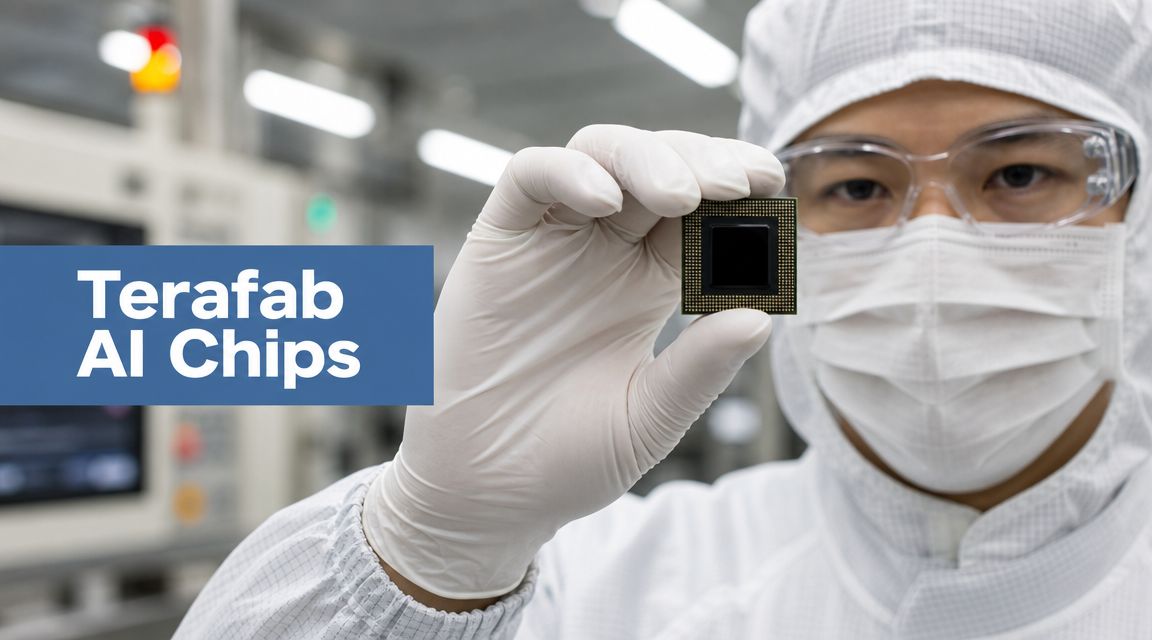
Last fact-checked: September 23, 2026. TeraFab plans to manufacture advanced logic and memory chips for Tesla and SpaceX applications. The official project identifies AI5 and AI6 for Tesla vehicles and Optimus robots, and D3 for SpaceX’s space-computing plans. Intel has joined the program, and Elon Musk has said the facilities intend to use Intel’s 14A manufacturing process.
These chips remain part of a product and manufacturing roadmap. Public sources do not yet provide verified TeraFab production benchmarks, yields, selling prices or complete architectures. Any performance table claiming exact TeraFab speed, cost or efficiency should therefore be treated cautiously.
Planned TeraFab chips
| Chip | Intended use | What is confirmed | What remains unknown |
|---|---|---|---|
| AI5 | Tesla Full Self-Driving and Optimus | Named on the official TeraFab site | Final specifications, manufacturing yield and TeraFab production date |
| AI6 | Future Optimus and AI workloads | Named on the official TeraFab site | Architecture, performance and production timetable |
| D3 | SpaceX computing in space | Presented as a space-oriented processor | Radiation qualification, package design, performance and launch timetable |
| Memory | High-bandwidth data access for AI workloads | Official materials include memory production and integration | Memory technology, supplier roles and production scale |
AI5 and AI6 for vehicles and robots
Tesla designs specialized processors for local inference: taking data from cameras and other systems and making decisions with limited delay. That matters in a vehicle or robot because a safety-critical decision cannot always wait for a remote data center.
The official TeraFab presentation associates AI5 with Full Self-Driving and Optimus, and AI6 with future Optimus workloads. It does not publish enough technical information to verify specific TFLOPS, TOPS-per-watt or cost claims. Those figures should not be inferred from the size of the factory.
If TeraFab succeeds, its practical advantage would be coordination. Tesla could align chip design, process choices, packaging and final product requirements more closely. The disadvantage is that Tesla and its partners would assume more of the difficult manufacturing work now handled by experienced suppliers.
D3 and space computing
Space hardware faces radiation, temperature and reliability requirements that differ from ordinary data-center systems. A processor intended for orbit may need design changes, error correction, shielding, packaging and qualification appropriate to its environment.
D3 is presented as the chip for SpaceX’s space-computing vision. Public descriptions do not yet establish its complete radiation-hardening method, final process, power efficiency or deployed configuration. The correct description is “planned space-oriented chip,” not a finished product with proven orbital performance.
Why memory and packaging matter
An AI processor cannot perform well if data arrives too slowly. Modern AI systems rely on high memory bandwidth and advanced packaging that places processors and memory close together. This reduces communication delays and energy used to move data.
TeraFab’s official material emphasizes logic, memory and advanced packaging under one roof. Tesla job postings also reference fabrication, packaging, testing and process engineering. That suggests the project is intended to control more than wafer fabrication alone.
However, “under one roof” is a strategic description. It does not prove that every material, tool, wafer stage or memory component will be produced internally. The semiconductor industry depends on specialized equipment and materials that will continue to come from outside suppliers.
Intel 14A explained
Intel 14A is a future manufacturing process in Intel’s foundry roadmap. The “14A” name refers to a 1.4-nanometre-class generation, although node labels no longer represent one physical transistor dimension. Musk said during a Tesla earnings call that TeraFab plans to use Intel 14A once the process and the project are ready.
This corrects a common outdated claim that TeraFab is simply a “2nm factory.” The project may use more than one process over its lifetime, and the final production plan can change. The important factors are process maturity, equipment readiness, design compatibility and yield.
How a TeraFab chip would be made
- Architecture and design: engineers define the chip’s functions and create the electronic design.
- Verification: the design is checked for logical, timing, power and manufacturing problems.
- Photomasks: production patterns are prepared for lithography.
- Wafer fabrication: repeated deposition, lithography, etch and implantation steps build transistors and interconnects.
- Wafer test: dies are screened before packaging.
- Advanced packaging: logic, memory and supporting components are connected in a package.
- Final test and qualification: finished devices are checked for performance and reliability in their intended use.
TeraFab’s claimed benefit is a tighter loop among these stages. A manufacturing constraint could be communicated to the design team quickly, while performance data from a vehicle, robot or space system could influence the next revision.
Does TeraFab compete with Nvidia?
Not directly in the same way that two chip products compete. Nvidia is primarily a fabless chip designer and computing-platform company. It creates GPUs, networking products and the CUDA software ecosystem, while external foundries manufacture its leading chips.
TeraFab is planned as a manufacturing and integration program serving affiliated companies. Tesla and SpaceX may design chips that reduce their need for some Nvidia hardware, but TeraFab does not begin with Nvidia’s broad product portfolio, customer base or software ecosystem.
See TeraFab vs TSMC and Nvidia for the complete business-model comparison.
Does TeraFab compete with TSMC?
TSMC is an established foundry that manufactures many different customer designs. TeraFab’s initial purpose is captive supply for SpaceX, Tesla and related programs. It could reduce their future reliance on outside foundries without becoming a broad merchant foundry.
The hardest gap is manufacturing experience. TSMC has decades of process data and yield learning. TeraFab’s vertical integration could improve design feedback, but it must still demonstrate repeatable production.
Claims that should not be treated as established facts
- Exact TeraFab chip performance or benchmark results.
- A guaranteed cost reduction compared with Nvidia or TSMC.
- A production date for AI5, AI6 or D3 from the large-scale fab.
- A claim that every component will be made internally.
- A claim that the fab already operates at 14A or any leading-edge node.
- A claim that space deployment has been technically qualified.
Milestones to watch
- Intel 14A process readiness and a finalized partnership structure.
- Installed lithography and process equipment at the research fab.
- First test wafers and disclosed yield progress.
- Qualified logic, memory and packaging flows.
- Named Tesla or SpaceX product using a TeraFab-manufactured chip.
- Volume-production data from the Grimes County facility.
Frequently asked questions
Is TeraFab making 2nm chips?
The current stated plan is to use Intel 14A, a future 1.4nm-class process. No large-scale TeraFab production has been verified.
Will TeraFab make Nvidia GPUs?
No such plan has been announced. The project is intended to make custom chips for Tesla and SpaceX-related applications.
What is the difference between AI5 and D3?
AI5 is associated with Tesla vehicles and robots. D3 is associated with SpaceX’s space-computing plans.
Why manufacture memory and packaging too?
AI performance depends on moving data efficiently. Integrating logic, memory and packaging can improve bandwidth, power efficiency and product-specific optimization.
Sources
- Official TeraFab products and manufacturing vision
- Tesla TeraFab engineering role
- Reuters: Intel joins TeraFab
- Reuters: Intel 14A and research-fab plan
For the broader project background, read what TeraFab is and how it is intended to work.
Related Posts
Previous Post
Next Post