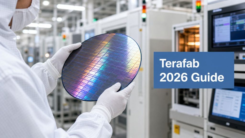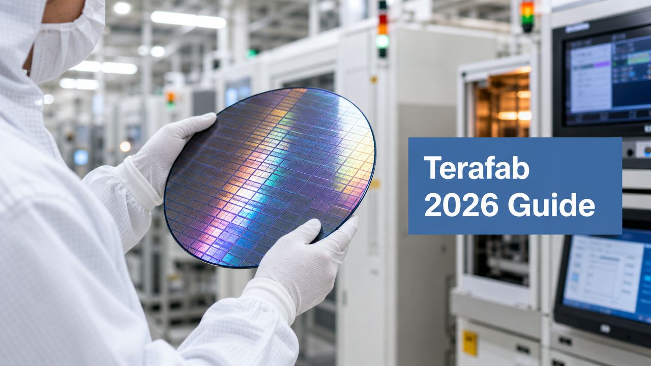
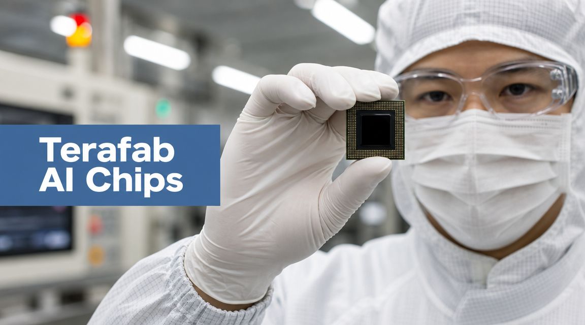
Terafab isn't just another company making AI chips. Think of it as something much bigger: a self-contained city built from the ground up for one purpose—cranking out the semiconductors that power modern AI. The whole idea is to control every single step of the process, from the initial design all the way to final testing, right there in Austin, Texas.
Imagine you wanted to build the world's best car. You wouldn't just design it; you'd build the steel mills, the engine plants, and the final assembly lines to own every piece of the puzzle. That’s the exact vision behind Terafab—a massive strategic play to get around the supply chain headaches that have plagued the tech industry and fuel the next wave of artificial intelligence.
At its core, the project is a direct answer to a huge supply problem. Back in March 2026, Elon Musk described it as a vertically integrated semiconductor complex meant to bring chip design, fabrication, and testing under one roof. The stated goal? To hit 1 terawatt of computing output per year. That's roughly 50 times the entire world's current AI computing output, a goal that helps explain the eye-watering initial investment estimates of $20 billion to $55 billion.
Most chip companies design their products and then send them off to someone else to be manufactured. Terafab is throwing that playbook out the window. The core idea is to own the entire process, which brings some huge advantages:
This is a big deal for anyone following technology. It could completely change the cost and speed of building and launching new AI systems. If you're new to the concepts behind the software these chips will run, our guide on machine learning for beginners is a great place to start.
Ultimately, Terafab is a massive bet that the biggest breakthroughs in AI will come from owning the factory, not just buying from it.
To really get what makes Terafab’s AI chips tick, you have to pop the hood. Forget the old way of making a single, massive, one-size-fits-all processor. Terafab is playing with high-tech LEGOs, and it’s a total game-changer.
The magic starts with chiplets. Think of these as small, independent blocks, each one a specialist at its job. One might be a math whiz, another a memory expert, and a third a communications guru. Instead of forcing one chip to do everything, Terafab combines these specialized chiplets into a single, powerhouse processor built for a specific AI task.
This modular approach gives them incredible flexibility. It means they can mix and match the perfect parts for any job, whether it's powering an autonomous car or training a massive language model—a level of customization that’s just not possible with traditional chip design.
But here’s where it gets really clever. Terafab doesn’t just lay these chiplets out side-by-side. They use 3D stacking, which is exactly what it sounds like: they build vertically. Imagine constructing a skyscraper of processing power instead of a sprawling single-story complex.
This vertical design has some serious perks:
By placing memory directly on the chip package—what’s known as on-package memory—Terafab basically builds a private, high-speed highway for data. This design choice sidesteps the traffic jams that slow down conventional systems, directly fueling faster and smarter AI.
This infographic paints a clearer picture of the sheer ambition behind the Terafab project and how these design choices fit into the bigger strategy.

As the visual shows, Terafab isn't just making chips. It's building an entire ecosystem to handle AI’s gigantic computing appetite.
Of course, to appreciate the genius of Terafab’s design, it helps to know a bit about the basic building blocks of any processor. This Server Scheduler's cores and threads guide is a great place to start. While you're at it, you might find it interesting how these advanced computing concepts sometimes echo ideas from another frontier technology, which we break down in our simple guide to quantum computing.
All the architectural wizardry in the world doesn't mean much if it can't deliver in the real world. So how do Terafab’s new chips actually stack up? When we talk about AI chip performance, it’s not just about one flashy number. It's a combination of raw power, energy efficiency, and how quickly it can churn through data.
Think of it this way. TFLOPS (Trillion Floating-Point Operations Per Second) is the raw horsepower of the chip. It’s a measure of sheer computational muscle. But just as important is TOPS/watt (Trillion Operations Per Second per Watt), which is more like a car's fuel efficiency. For massive data centers, getting more performance without a sky-high energy bill is the name of the game.
Terafab isn't just trying to play in the same sandbox as NVIDIA and Google; it's trying to build a whole new one. The goal seems to be completely upending the economics of AI compute. Initial projections suggest they have a fighting chance.
Of course, raw power is just one piece of the puzzle. Understanding a chip's ability to handle massive, continuous streams of data—its throughput—is just as vital. This is something that gets a great breakdown from the team at Supagen on AI throughput.
Based on what we know, here’s a look at how Terafab's projected specs for 2026 measure up against the industry titans.
This table gives a clear snapshot of the different strategies at play. Terafab is betting on hyper-specialization, while NVIDIA continues to dominate the general-purpose market.
| Feature / Metric | Terafab AI Chip (Projected) | NVIDIA Blackwell B200 | Google TPU v6 (Projected) |
|---|---|---|---|
| Primary Focus | Hyper-specialized for Tesla, xAI, SpaceX | General-purpose AI & HPC | Google's internal AI workloads |
| Target Power Use | Claims one-third the power of Blackwell | High-performance, power-intensive | Optimized for efficiency at scale |
| Manufacturing Cost | Aims for 10% of Blackwell's cost | High, due to advanced fabless model | Proprietary, optimized for Google Cloud |
| Key Advantage | Vertical integration, cost control | CUDA software ecosystem, broad adoption | Deep integration with Google's stack |
The key takeaway here is the strategic split. NVIDIA builds incredibly powerful, do-it-all GPUs that appeal to a wide customer base, backed by its unbeatable CUDA software. Terafab, on the other hand, is laser-focused on vertical integration and cost control. If their claims about performance, power, and cost hold up, the implications are huge.
It's a bold move, playing a different game than the established leader. We took a closer look at NVIDIA's own long-term strategy in our analysis of how Jensen Huang will become HR for AI agents.

This focus isn't just academic; it translates to very real advantages. For a company like xAI, it could slash the time it takes to train a next-gen large language model from months to mere days. For a Tesla on the road, it means processing more complex sensor data to make safer, split-second decisions.
Ultimately, the performance numbers aren't just for a spec sheet—they are the fuel for the next major leap in AI.
Incredible hardware is only half the story. Without the right software, even the most powerful chip is just a fancy piece of silicon. This is where Terafab's software ecosystem comes in, acting as the critical translator between a developer's code and the chip's raw power.
This ecosystem is built around the Tera-Stack, a complete software suite with its own SDK, compiler, and libraries. Think of it as the operating system for Terafab's hardware, designed from the ground up to get every last drop of performance out of the chips.
The Tera-Stack isn’t an afterthought; it’s the result of a strategy called hardware-software co-design. Instead of building the chip and then figuring out how to program it, Terafab's engineers developed both at the same time. This ensures the software speaks the hardware's native language, eliminating the bottlenecks you see with a one-size-fits-all approach.
What does this mean for a developer? Simplicity. The Tera-Stack is designed to feel familiar, neatly translating code from the most popular AI frameworks into hyper-specific instructions the hardware can crush.
| Framework Integration | How Tera-Stack Handles It | The End Result |
|---|---|---|
| TensorFlow | The compiler automatically optimizes TensorFlow graphs for Terafab’s unique chiplet design. | Your existing AI models run with incredible speed on specialized hardware, without a major rewrite. |
| PyTorch | Custom libraries give you direct, low-level access to Terafab’s on-package memory and compute units. | You can fine-tune the most demanding parts of your code while staying within the PyTorch environment you already know. |
This co-design approach is Terafab’s answer to a crucial question: how do you convince the world’s best AI programmers to adopt a brand-new platform? The answer is by making the transition as smooth as possible, abstracting away the hardware complexity while unlocking its full power.
Let's be realistic: a new platform always comes with a learning curve. But Terafab is betting that the mind-bending performance gains are worth it. The key to winning over developers will be rock-solid documentation, a helpful community, and great debugging tools.
By integrating with frameworks developers already use every day, Terafab is making it easier for them to focus on what really matters: building the next generation of AI. To get a better sense of what's possible, you can learn more about generative AI business applications in our detailed guide.
So, where will these powerful Terafab AI chips actually be put to work? Their first job is to become the new engine for Elon Musk's most ambitious projects. The initial applications are zeroed in on solving some of the toughest problems in AI and engineering today.
The new chips are slated to power the next generation of Full Self-Driving (FSD) software. For FSD, this means crunching a massive amount of real-world sensor data faster than ever. For example, a Terafab-powered car could analyze video from all eight cameras simultaneously, identify hundreds of objects, predict their trajectories, and make a driving decision in milliseconds—a level of processing that allows for more human-like reactions to complex urban environments.
At the same time, xAI will be using Terafab’s hardware to train its next wave of large language models. A real-life scenario would involve training a new model like "Grok 3" on a dataset ten times larger than its predecessor. With current hardware, this could take six months and cost hundreds of millions. With a dedicated cluster of Terafab chips, the goal is to cut that training time to just three weeks, dramatically accelerating the pace of AI discovery.
Even SpaceX gets a piece of the action. The D3 chip variant, built tough for the extreme conditions of space, is designed for real-time data processing on Starlink satellites and Starship missions. For instance, a network of D3-equipped Starlink satellites could process Earth observation imagery in orbit, detecting wildfires or tracking maritime activity in real-time, and beaming down only the critical alerts instead of terabytes of raw data. This opens the door to a massive, orbiting data center that could perform AI tasks in space, running on virtually limitless solar power.

While the first priority is clearly internal, the sheer scale of the Terafab project points to a much bigger game. With a planned production volume that goes way beyond what his own companies need, Musk could eventually take a shot at the cloud computing market. Offering Terafab's processing power as a service would put it in direct competition with giants like AWS, Google Cloud, and Microsoft Azure. You can see how these ventures fit into his broader financial strategy in our article on how he became so rich.
The strategic play is clear: solve the immediate, immense compute needs of the internal empire first, then use that scaled-up production to disrupt the broader market.
Of course, measuring the payoff for such huge AI projects is critical. For any company thinking about adopting powerful new hardware, centralizing AI automation metrics is essential to justify the massive investment. Terafab’s success won’t just be about making chips; it will be about proving their worth in these high-stakes applications.
The big question everyone's asking is whether Terafab is a true "NVIDIA killer" or just a specialized tool for its own ecosystem. The answer isn't simple. Terafab is taking a completely different path by vertically integrating—controlling everything from chip design all the way to manufacturing.
This is a huge departure from the norm. For years, the market has run on a division of labor: companies like NVIDIA design the chips, and foundries like TSMC build them. Terafab is tearing up that playbook, bringing the entire process in-house to gain total control over its supply chain and sidestep the bottlenecks that have plagued the industry.
Of course, this is a massive gamble. Building a world-class semiconductor factory from the ground up costs billions and requires near-perfect execution. But if they pull it off, the reward is equally massive. Terafab could fundamentally alter the cost of building large-scale AI.
Early reports suggest Terafab's custom chips, like the AI5 processor, could be made for just 10% of the cost of a competing NVIDIA Blackwell chip. On top of that, they're expected to use only a third of the power—a game-changer for data centers where energy bills are a massive operating expense.
This one-two punch of lower cost and higher efficiency is Terafab's secret weapon. It’s not just about building a faster chip; it’s about making huge AI models financially sustainable for the first time.
While Terafab is betting on its closed, vertically-integrated model, its rivals have different strengths. NVIDIA's dominance isn't just about hardware; it's built on its CUDA software platform, a mature ecosystem with a gigantic and loyal developer base. That software "moat" is incredibly tough to cross.
Here’s how the competitive landscape stacks up:
| Competitive Factor | Terafab | NVIDIA |
|---|---|---|
| Business Model | Vertically integrated (design & fab) | Fabless (design only) |
| Primary Strength | Cost control and supply chain ownership | CUDA software ecosystem and market adoption |
| Target Market | Internal use (Tesla, xAI) | Broad, general-purpose AI market |
| Key Differentiator | Hyper-specialization for specific tasks | Versatility and developer ecosystem |
In the end, Terafab isn't just trying to beat NVIDIA on performance benchmarks. It's proposing an entirely new way to build and pay for AI infrastructure. Its real impact won't be measured in TFLOPS, but in how it forces the rest of the market to rethink their own strategies from the ground up.
Terafab is a massive, vertically integrated semiconductor project initiated by Elon Musk. Its goal is to design, manufacture, and test AI chips entirely in-house at a single, massive facility in Austin, Texas. Think of it as a dedicated "city for chips" built to power companies like Tesla, xAI, and SpaceX.
The core difference is specialization vs. versatility. An NVIDIA GPU is a powerful, general-purpose tool, like a high-end Swiss Army knife. A Terafab chip is a custom-designed scalpel, built for a very specific set of AI tasks within Musk's ecosystem. This specialization allows for extreme optimization in performance and cost, which isn't possible with a one-size-fits-all chip.
Initially, yes. The primary goal is to supply the immense computational needs of Tesla's self-driving AI, xAI's language models, and SpaceX's in-orbit processing. However, the project's enormous planned output (1 terawatt annually) far exceeds internal needs, suggesting a long-term plan to sell compute power as a cloud service, competing with AWS, Google Cloud, and Azure.
Execution. Building a leading-edge semiconductor fabrication plant is one of the most complex and expensive engineering feats in the world. The project faces immense technical and logistical hurdles, from achieving high manufacturing yields (the percentage of working chips per wafer) to managing a multi-billion dollar construction timeline. Any significant delay or mistake could jeopardize the entire venture.
It means controlling the entire supply chain. Instead of designing a chip and outsourcing manufacturing to a company like TSMC (the "fabless" model), Terafab will do everything under one roof. This provides complete control over the timeline, cost, and design, eliminating reliance on third-party suppliers and their potential bottlenecks.
Early projections claim that a Terafab-produced chip could be manufactured for as little as 10% of the cost of a comparable high-end NVIDIA chip. This is achieved by eliminating the foundry's profit margin, optimizing the design for a single manufacturing process, and creating chips that are "good enough" for their specific task rather than over-engineered for general use.
The Tera-Stack is the proprietary software suite designed to unlock the hardware's potential. It includes a compiler, libraries, and a software development kit (SDK) that translates code from popular AI frameworks like TensorFlow and PyTorch into instructions that Terafab's unique chiplet architecture can execute with maximum efficiency.
You likely won't buy a consumer device with a "Terafab Inside" sticker. Instead, you'll experience its impact through the services it powers. This includes more advanced Full Self-Driving capabilities in Tesla cars, more powerful and responsive AI models from xAI, and new capabilities from SpaceX's Starlink. The first tangible effects are expected to emerge around the 2027-2028 timeframe.
Directly, it will be very difficult. NVIDIA's CUDA platform has a 20-year head start and is deeply entrenched in the AI research and development community. Terafab's strategy isn't to replace CUDA everywhere. Instead, it aims to create a closed ecosystem where the extreme performance and cost advantages of its hardware/software combination are so compelling for its internal projects that using anything else becomes illogical.
The name is a combination of two key concepts: "Tera" and "Fab." "Tera" refers to the project's immense scale, with a target of producing one terawatt of AI compute power annually. A terawatt is a trillion watts. "Fab" is industry shorthand for a semiconductor fabrication plant, the factory where chips are made. Together, "Terafab" signifies a fabrication plant of unprecedented scale.
At Everyday Next, we're dedicated to breaking down the complex technologies shaping our world. From AI breakthroughs to investment trends, we provide the insights you need to stay ahead. Explore our latest articles and join the conversation.