Terafab Pros and Cons Explained: AI Chip Fab Impact 2026
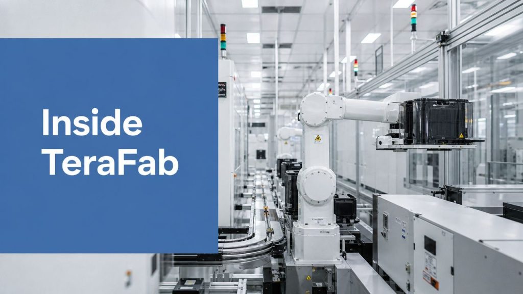
A factory that aspires to 1 million 300mm wafer starts per month from a single site would be operating at a scale that one report says is roughly 70% of TSMC's current total global output (Metatrends). That one figure changes how Terafab should be understood. This isn't a normal fab story. It's an attempt to move control of AI-era compute supply away from the existing foundry system and into one vertically integrated industrial stack.
That's why simple “bullish vs bearish” takes miss the point. Terafab matters because it sits at the intersection of semiconductors, power infrastructure, robotics, autos, defense-adjacent supply resilience, and capital markets. It promises faster custom chip development and tighter control over supply. It also runs straight into the hardest realities in manufacturing: process maturity, yield learning, tooling bottlenecks, and economics that may look more like a national industrial program than a corporate expansion.
If you follow AI infrastructure, autonomous systems, or the companies in Elon Musk's orbit, Terafab is worth studying for the same reason readers track shifts in generative AI business applications. The strategic issue isn't just what AI can do in software. It's who controls the silicon when demand outruns available supply.
Table of Contents
- An Introduction to the Terafab Ambition
- What Is the Terafab Vision
- The Strategic Pros of Building a Terafab
- The Significant Cons and Execution Risks
- Market Impact and Economic Reality
- Actionable Takeaways and Future Outlook
- Frequently Asked Questions About Terafab
An Introduction to the Terafab Ambition
A leading-edge chip fab can cost tens of billions of dollars before it produces a meaningful volume of usable chips. That number is the right starting point for Terafab, because the project only makes sense if its promised strategic upside is large enough to outweigh the physics, capital intensity, and long build times of semiconductor manufacturing.
The useful way to frame this section is not around branding or corporate ambition. It is around feasibility. Semiconductor fabs are unusual industrial assets because scale alone does not guarantee output, yield, or cost competitiveness. A company can spend heavily and still end up with a facility that is late, underutilized, or dependent on outside suppliers for tools, materials, packaging, and IP.
That is why Terafab deserves analysis as a capital allocation question first. If a company wants tighter control over the chips that power AI servers, autonomous systems, and other specialized products, building fabrication capacity may look attractive. The harder question is whether owning more of the production chain produces better economics than securing supply through long-term foundry agreements, co-design partnerships, and packaging capacity. Readers tracking practical generative AI business applications should pay attention to this distinction, because advanced AI products depend on chip supply that is reliable, not just theoretically in-house.
What makes this different from a routine expansion
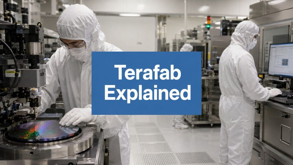
A semiconductor fab works like a tightly synchronized chain of laboratories. Lithography, deposition, etch, metrology, and packaging each have their own bottlenecks, and a delay in one stage can reduce output across the whole site. That makes a Terafab-style plan more complex than adding floor space or buying extra server racks.
The economic implication is easy to miss. In software, one successful product can scale fast with limited marginal cost. In chip manufacturing, each new increment of capacity requires more tools, more utilities, more process control, and more operational discipline. The result is a steep feasibility gap between a compelling vision and a factory that can repeatedly ship chips at commercial yields.
For investors and industry watchers, the signal to watch is not the announcement itself. It is whether the project can convert capital into stable production, on time, at yields and costs that justify building it at all.
What Is the Terafab Vision
A proposed output measured in the hundreds of thousands to millions of wafer starts per month sounds less like a normal factory plan and more like a bid to compress a large share of the global semiconductor supply chain into one location. That scale is the point of the Terafab idea. It is not merely about owning a chip plant. It is about trying to internalize design, manufacturing, and possibly downstream packaging around a narrow set of AI and embedded computing needs, as noted earlier.

Vertical integration in plain English
Semiconductor production works less like assembling laptops and more like running an airport where every runway, gate, and maintenance crew must stay synchronized. Chip design, wafer processing, testing, advanced packaging, power delivery, water treatment, and software all interact. Bringing more of that chain under one owner can shorten feedback loops, but only if each stage performs at commercial quality and yield.
That is the core meaning of the Terafab vision. It treats chips as strategic infrastructure, not as components bought from a catalog. The logic is familiar to readers following AI agents in the enterprise and the shift toward custom AI infrastructure. Generic capacity is useful until supply becomes scarce, product requirements become specialized, or timing matters more than nominal unit cost.
The concept also fits workloads that are repetitive, power-constrained, and tightly tied to one company's products. Autonomous driving inference, robotics control, edge AI, and machine vision all benefit more from purpose-built silicon than broad consumer computing does. The engineering tradeoffs resemble designing AI vision systems, where the best result often comes from matching the model, sensor, and deployment environment instead of optimizing any one piece in isolation.
What the vision implies
The non-obvious part is what Terafab assumes about the future. A company does not pursue this kind of integration unless it expects outside foundry access, packaging capacity, or strategic control to become a limiting factor.
That makes Terafab less a manufacturing story than a thesis about bottlenecks. If management believes future AI products will be constrained by chip availability, power budgets, or process customization, then owning more of the stack can look rational. If those constraints ease, the same project starts to look like an attempt to carry the cost and complexity of a national-scale industrial system on a single corporate balance sheet.
So the vision is ambitious in a very specific way. It aims to turn semiconductor supply from an external dependency into an internal operating capability. The appeal is clear. The harder question is whether the economics and physics of chipmaking allow that ambition to translate into repeatable output rather than a compelling narrative.
The Strategic Pros of Building a Terafab
Semiconductor manufacturing rewards control, but only at extraordinary scale. That tension defines the upside case for Terafab.
The strategic appeal starts with one practical advantage. A company that designs chips and controls more of the production path can align transistor choices, packaging, thermal limits, software, and product timelines around its own workloads instead of a foundry's average customer. In plain terms, it is the difference between renting compute on a crowded schedule and building a private power plant for a factory that runs day and night. The first is flexible. The second can be far more efficient if utilization stays high enough.
Why private chip supply can create real advantages
For AI, robotics, and embedded systems, specialization matters more than broad compatibility. A training accelerator, a self-driving inference chip, and a robot control processor do not need to excel at every computing task. They need to perform a narrow set of operations with low latency, controlled heat, and predictable power draw. Bringing design and manufacturing into a tighter loop can improve performance per watt because the chip is tuned for a defined job rather than for the wider merchant market.
That benefit is easy to overstate, but it is real.
A closer coupling between sensing, silicon, and software also shortens engineering feedback cycles. If a perception team finds that a camera pipeline needs a different memory layout or a robotics stack needs lower latency on one operation, those changes can feed back into chip and packaging decisions faster when fewer outside handoffs are involved. The same systems logic appears in adjacent fields such as designing AI vision systems, where the best results come from fitting hardware, models, and operating conditions together rather than optimizing each part in isolation.
There is also a supply chain argument. The automotive chip shortage showed how quickly outsourced semiconductor dependence can become a production constraint. For a company whose products depend on steady access to custom silicon, internal capacity can reduce exposure to foundry queues, export controls, and supplier priority decisions. It does not remove those risks, because tools, materials, and packaging still come from global networks, but it can reduce one important layer of dependency.
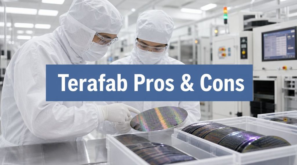
Terafab at a glance
| Pros (The Vision) | Cons (The Reality) |
|---|---|
| Tighter control over chip supply | Fabrication is one of the hardest industries to enter |
| Faster design-to-manufacturing feedback | Delays in process readiness can stall the whole roadmap |
| Better performance-per-watt for narrow workloads | Parallel technical paths raise complexity and burn rate |
| Reduced dependence on outside foundries | Workforce and operational depth may be insufficient |
| Potential insulation from supply chain shocks | Economic feasibility is deeply uncertain |
What the upside means in business terms
- Higher strategic control: Silicon supply becomes part of product planning rather than an external constraint imposed by another company's capacity allocation.
- Faster iteration on specialized products: Chip teams and product teams can revise around the same bottlenecks instead of waiting through long vendor cycles.
- Better economics, if utilization is sustained: A dedicated fab can make sense when demand is large, stable, and concentrated in a few high-value product lines.
- Stronger positioning in automation-heavy industries: Companies that pair custom silicon with manufacturing scale can shape their own cost curves, a pattern visible in broader reporting on industrial robot production growth and the new automation cycle.
The non-obvious conclusion is that Terafab's best argument is less about prestige and more about bottleneck ownership. If future AI and robotics markets are constrained by chip availability, energy efficiency, and product-specific optimization, then more internal manufacturing control could become a competitive advantage with real economic value. If those constraints ease, many of these strategic benefits shrink quickly, because the same integration that improves coordination also fixes the company to a far heavier industrial cost base.
The Significant Cons and Execution Risks
Semiconductor manufacturing punishes optimism faster than almost any other industry. A company can have a plausible strategic reason to internalize chip supply and still fail on process control, hiring, equipment timing, or economics.

The node dependency problem
One reported risk is dependence on Intel's 14A process and the timing of its Process Design Kit, or PDK (TradingKey). The PDK is the foundry's manufacturing rulebook. It defines what designers can build, how dense circuits can be, which libraries are valid, and what reliability limits apply. If that rulebook arrives late, changes materially, or remains immature, design teams cannot finalize layouts with confidence.
That matters because chip schedules are sequential. Architecture feeds layout. Layout feeds verification. Verification feeds tape-out. Tape-out feeds fabrication, packaging, and system integration. A delay at the process level can push the whole chain back by months, and late-stage fixes are expensive because they occur after engineering teams have already committed headcount and design choices.
The same reported analysis also points to scope risk, compressed timelines, and staffing pressure. Those problems reinforce each other. A fab project is not a single engineering program. It is dozens of tightly linked programs that have to mature at roughly the same speed.
Manufacturing is harder than design
Designing a competitive chip and manufacturing it at scale are different businesses. One rewards architectural insight and software tools. The other rewards contamination control, yield learning, equipment uptime, materials logistics, and process discipline across thousands of steps.
A useful analogy is aircraft production. Drawing a better jet is hard. Producing that jet safely, repeatedly, and profitably at industrial volumes is a separate achievement. Advanced semiconductors are similar, except the tolerances are measured in nanometers and defects that cannot be seen by the naked eye can destroy wafer output.
That is the core execution risk. If Terafab is framed mainly as an extension of product ambition, investors can miss the fact that fabs are operating systems for physics, chemistry, and statistics.
The physical bottlenecks are broader than silicon
Even a technically sound fab plan would face constraints outside the fab walls. Chips only create business value once they are packaged, paired with memory, connected to power delivery, cooled, assembled into systems, and deployed into facilities with enough electricity and thermal management. A wafer start is not a finished compute cluster.
This point gets lost in headline narratives. Semiconductor capacity is only one layer of the stack. Advanced packaging has become a bottleneck. High bandwidth memory is constrained. Power infrastructure takes years to expand. Grid access and industrial policy also shape project timing, especially in a market affected by new tariffs and trade rules for 2025.
So the primary question is not whether a fab can produce chips. It is whether the surrounding supply chain can absorb them at the same pace.
Time is a risk factor, not just a project variable
A long learning curve changes the economics of the entire vision. If ramp-up takes years longer than expected, the target market may shift before the manufacturing base is mature. Process nodes evolve. AI hardware demand changes shape. Competitors sign supply agreements, improve their own custom silicon, or lock up packaging capacity.
This is why execution risk in semiconductors is more than schedule slippage. Delay can erase the original strategic logic. A fab that reaches useful scale after the market bottleneck has moved may still be technically impressive and financially disappointing.
The sharpest downside, then, is not that Terafab could underperform its most ambitious claims. It is that the project may succeed in building expensive industrial capability while missing the specific window that made that capability attractive in the first place.
Market Impact and Economic Reality
The most important question isn't whether Terafab sounds strategic. It's whether the economics support the scale implied by the vision.

The feasibility gap
One Bernstein analysis, as reported by Tom's Hardware, estimates that reaching Terafab's stated 1 terawatt output goal would require 142 to 358 individual fabs at a cost of well north of $4 trillion, compared with a headline project budget of about $20 billion to $25 billion (Tom's Hardware).
That gap is the heart of any honest Terafab pros and cons explained analysis. It suggests that two very different ideas may be getting blended together:
- A realistic effort to internalize more semiconductor capability.
- A stated end-state so large that it resembles a multi-decade industrial mobilization.
If you separate those, the discussion gets clearer. A partial win might still matter commercially. A full realization of the grandest claims could be economically irrational under current semiconductor cost structures.
What this means for investors and supply chains
For investors, the main takeaway is that Terafab shouldn't be modeled like a normal capex line item. It behaves more like an option on strategic control. The option may prove valuable even if the original scale target doesn't.
For the broader market, the project still matters because it signals dissatisfaction with the current foundry dependence model. If large AI-heavy firms increasingly want dedicated or semi-dedicated supply, equipment vendors, packaging providers, memory suppliers, and software tool companies could all gain influence. Public market interest in those second-order beneficiaries may at times be more grounded than enthusiasm for the flagship concept itself. That's a useful lens when evaluating themes such as AI infrastructure investing.
Analyst's view: The biggest risk may not be that Terafab fails completely. It may be that it succeeds just enough to consume enormous capital without ever matching the economics of established foundries.
The deeper implication is that the business case depends on scale discipline. The rational version of Terafab may be smaller, narrower, and more specialized than the headline vision.
Actionable Takeaways and Future Outlook

Terafab looks strongest as a partial vertical-integration strategy and weakest as a literal interpretation of its most ambitious scale claims. That's the balanced conclusion. The strategic logic is credible. The execution and economic hurdles are severe.
Who should watch what
- Investors: Watch for evidence of narrower milestones rather than grand capacity claims. Process partnerships, tooling progress, packaging plans, and realistic ramp sequencing matter more than slogans.
- Engineers and operators: Skills tied to process integration, EDA workflows, packaging, yield analysis, and power-aware AI hardware become more valuable if companies keep pulling semiconductor work in-house.
- Supply chain observers: Focus on who benefits even if Terafab stays incomplete. Equipment, testing, memory, packaging, and foundry-adjacent infrastructure may capture value first.
A practical way to think about the future is this: the most plausible success case isn't “a company recreates TSMC overnight.” It's “a company builds enough in-house capability to improve bargaining power, accelerate custom silicon programs, and secure supply for a few critical products.”
For a broader visual explainer on the topic, this video is a useful companion.
The best alternative for firms without extreme capital tolerance is usually not a terafab-scale moonshot. It's some mix of chiplets, foundry partnerships, advanced packaging, and tightly scoped custom silicon. That path won't generate the same headlines, but it often produces better economics.
Frequently Asked Questions About Terafab
Below are the most practical questions readers still ask after looking at the vision, the risks, and the economics.
| Question | Answer |
|---|---|
| What is Terafab in simple terms? | It's a proposed large-scale, vertically integrated semiconductor manufacturing program aimed at securing custom chip supply for AI-heavy products rather than relying fully on external foundries. |
| Why is vertical integration such a big deal here? | Because it can shorten the feedback loop between chip design, manufacturing, testing, and deployment. In semiconductor programs, those handoffs often determine schedule risk. |
| Is Terafab mainly about Tesla cars? | No. The strategic case presented around the project extends beyond vehicles to AI-heavy products such as robotics and space-based systems, based on the reporting cited earlier. |
| What is the biggest upside? | Control. A company with internal chip capability can prioritize its own products, tune silicon for narrow workloads, and reduce exposure to external supply bottlenecks. |
| What is the biggest technical risk? | Process readiness. The earlier cited market analysis flags dependency on Intel's 14A node and a delayed PDK as a major risk because those issues can freeze layout, verification, and tape-out. |
| Why do analysts question the project's feasibility? | Because fabs require specialized equipment, highly controlled facilities, experienced teams, and long learning cycles. Those constraints don't disappear just because demand is real. |
| Is the power requirement a serious issue? | Yes. One analysis argues that the stated compute ambition runs into current physical constraints around terrestrial power availability, which is why off-planet compute appears in some discussions of the concept. |
| Does Terafab need to reach its largest claims to matter? | No. A smaller, more focused version could still improve supply security and internal chip development speed. Partial success may be commercially meaningful even if the broadest vision is unattainable. |
| Who could benefit even if Terafab never reaches full scale? | Companies involved in semiconductor equipment, packaging, memory, testing, design tools, and process integration could benefit from any serious move toward more domestic or captive chip capacity. |
| What should readers watch next? | Evidence of disciplined execution. Partnerships, process milestones, workforce buildout, packaging strategy, and realistic production sequencing will tell you more than headline ambition. |
Terafab is fascinating because it forces one uncomfortable conclusion. The AI race isn't only about models and software. It's increasingly about industrial capacity, energy, and who can lock down the physical means of computation. That makes this story bigger than one company and more important than the hype cycle around it.
If you like analysis that connects technology, markets, and real-world decision-making, explore more from Everyday Next. It's a strong resource for readers who want practical insight on AI, investing, innovation, and what these shifts mean for everyday life.
Related Posts
Previous Post
Next Post