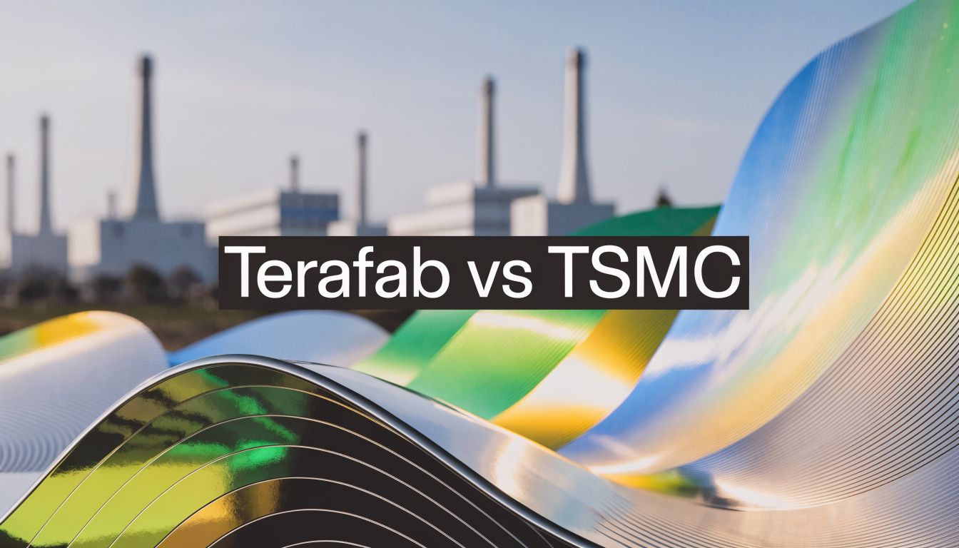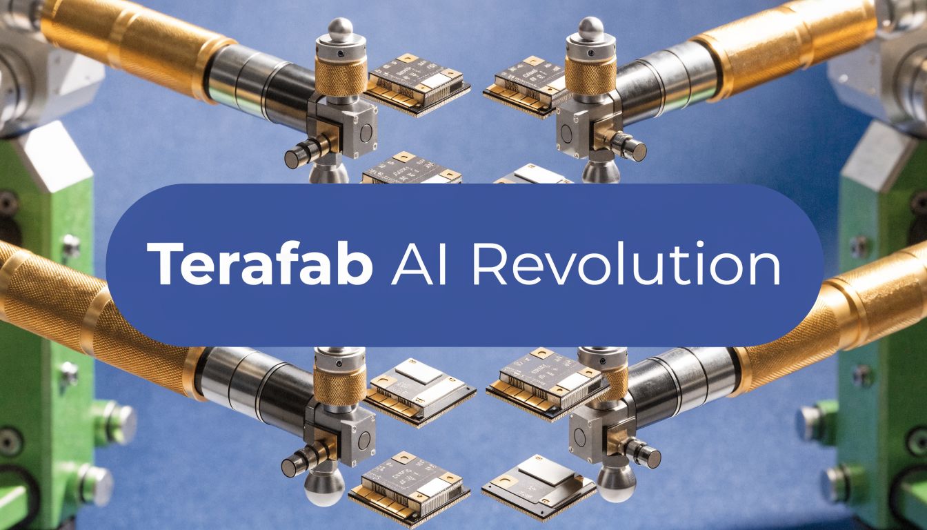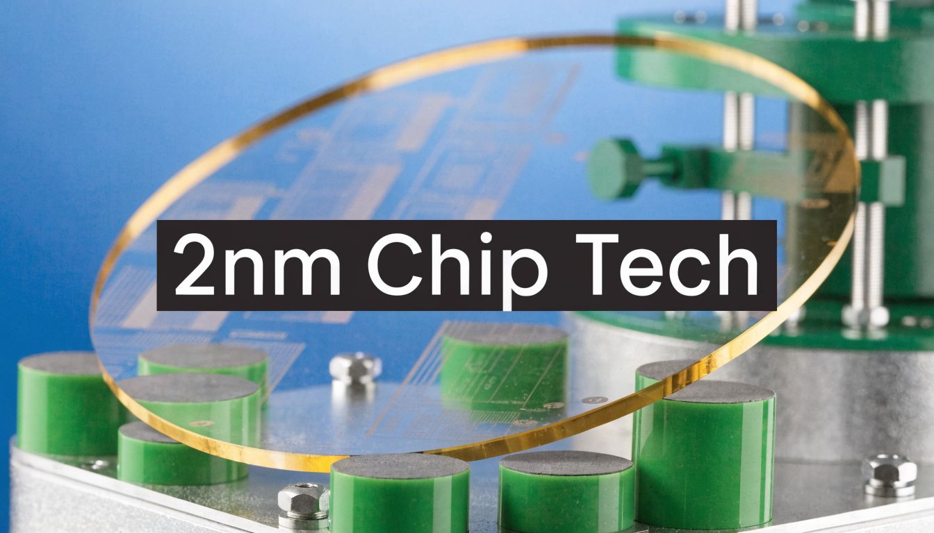
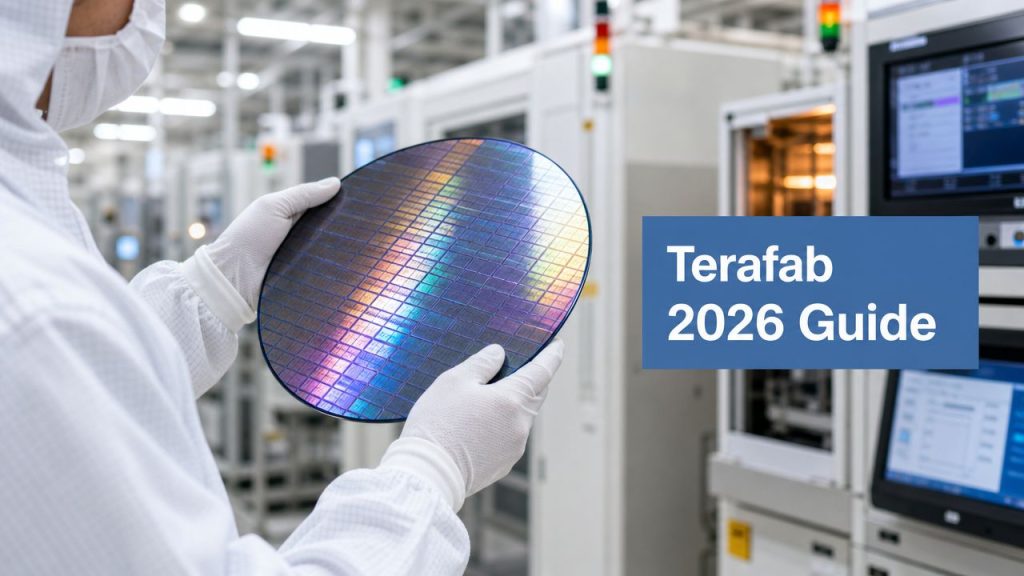
TeraFab 2nm Chip Technology Details Explained
A factory aimed at delivering AI compute on the scale of a terawatt per year would not be a normal fab expansion. It would signal an attempt to reorganize how advanced chips are designed, built, packaged, and consumed under one command structure.
That is why TeraFab matters.
The headline is 2nm, but the strategic question sits one layer deeper. Gate-all-around transistors matter because they give engineers tighter control over current at very small dimensions, much like wrapping a pipe with more insulation to reduce leakage. EUV matters because it lets manufacturers print finer features with fewer patterning steps, which can improve both yield and cycle time. Yet those process gains become much more valuable when the same organization also controls packaging, system design, software workloads, and large internal demand from vehicles, robotics, AI training, and aerospace.
This makes TeraFab more than a foundry story. It is a vertical integration story built on semiconductor physics.
For investors and tech leaders, the disruption is not just faster chips. It is the possibility that one company group could shrink the distance between transistor innovation and shipped products. If that happens, TeraFab would pressure the standard industry model, where design, fabrication, advanced packaging, and deployment often sit in different companies with different incentives and timelines. The result could be a shift in bargaining power across the semiconductor field, especially if manufacturing scale and captive demand reinforce each other.
Table of Contents
- What Is TeraFab and Why Does It Matter
- Inside TeraFab's 2nm Architecture
- Expected Performance and Power Gains
- The Unprecedented Scale of TeraFab Manufacturing
- How TeraFab Compares to TSMC Samsung and Intel
- Roadmap Costs and Supply Chain Upheaval
- What TeraFab Means for Products and Investors
- Frequently Asked Questions About TeraFab Technology
- 1. What is TeraFab in simple terms
- 2. What does 2nm mean here
- 3. Why is GAA important
- 4. Is TeraFab already producing chips at scale
- 5. Why are investors paying attention
- 6. How does TeraFab differ from TSMC
- 7. What products could benefit first
- 8. What is the biggest execution risk
- 9. Why does advanced packaging matter so much
- 10. Could TeraFab reshape the chip industry
What Is TeraFab and Why Does It Matter
A modern AI training cluster can consume more capital than many factories. TeraFab appears designed to answer that pressure with a different model: treat advanced chips as captive industrial capacity, then route that capacity across vehicles, robots, data centers, and aerospace systems under one corporate umbrella.
That framing is more important than the factory name. A conventional fab expands supply for the wider market. TeraFab, as described publicly, points to something narrower and more disruptive: a vertically integrated silicon pipeline tied directly to Musk-aligned products and platforms. The project's significance lies in its potential to shift control over compute from external suppliers to the company shipping the end systems.
The strategic logic is straightforward. If Tesla, xAI, SpaceX, and related programs depend on outside foundries, advanced packaging houses, and memory partners, product schedules remain exposed to the priorities and capacity constraints of other firms. If the same ecosystem can design chips, manufacture them, package them, and deploy them internally, semiconductor supply stops being just a procurement issue. It becomes a source of operating speed.
That distinction will matter more over the next few years than many executives assume. Across the broader top tech trends shaping 2025 and beyond, the recurring theme is not just better AI models or smarter devices. It is tighter control of the stack underneath them.
Why this isn't just another chip project
The standard semiconductor model splits responsibility across several companies. One firm designs the processor. Another fabricates the wafer. A third handles advanced packaging. The device maker then adjusts product plans around whatever supply is available.
TeraFab aims to compress those steps into one coordinated system.
For investors, that changes the question. The issue is no longer only whether a 2nm chip can outperform rivals on a benchmark. The bigger issue is whether integrated chip supply lets one ecosystem iterate products faster, absorb shortages better, and protect margins that would otherwise be shared with foundries and packaging vendors.
A simple analogy helps. EUV lithography is the tool that draws microscopic circuit patterns using extremely short-wavelength light, like using a finer pen to sketch denser city streets. GAA transistors, covered in the next section, improve how each switch controls electrical flow, more like replacing a leaky valve with one that seals from every side. Put those two pieces inside one vertically coordinated manufacturing plan, and the benefit is not only a better chip. It is a shorter path from design choice to commercial product.
Why tech leaders should pay attention
If TeraFab works as intended, competition changes shape. The relevant comparison is no longer just node against node or chip against chip. It becomes supply certainty, design feedback speed, packaging control, and deployment scale, all inside the same corporate system.
That has implications beyond Tesla. Merchant chip suppliers could face a customer that increasingly builds for itself. Foundries could face a high-volume buyer that turns into a partial competitor. Governments could see one more example of semiconductor capability concentrating around companies that combine software, hardware, manufacturing ambition, and access to large end markets.
For Musk's ecosystem, the appeal is clear. Cars, humanoid robots, AI training clusters, and spacecraft do not need identical chips, but they do benefit from shared process technology, packaging know-how, power management, and internal demand planning. For the global semiconductor power balance, that is the more interesting signal. TeraFab suggests the next contest may center less on who can design the best individual processor and more on who can internalize the bottlenecks that determine how fast advanced systems reach the field.
Inside TeraFab's 2nm Architecture
The simplest mistake in semiconductor analysis is to assume “2nm” tells you most of what you need to know. It doesn't. Modern node names are partly branding shorthand. The deeper issue is how the transistor is built and how reliably that design can be manufactured at scale.
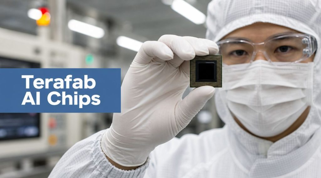
TeraFab's reported 2nm approach centers on Gate-All-Around, or GAA, nanosheet transistors. According to Tesery's report on the architecture and claimed benefits, this design is intended to deliver 30-40% higher transistor density, a 25-35% performance uplift at the same power level, and 60-75% lower leakage currents compared with 3nm FinFET baselines.

Why 2nm matters less than the transistor design
For years, FinFET transistors carried the industry. They improved control by raising the transistor channel into a fin-like shape so the gate could wrap around more of it. But as features shrink, controlling current leakage gets harder. Electrons start behaving less like obedient commuters and more like people slipping through side doors.
GAA is the next answer. A simple analogy helps. FinFET is like pinching a hose from several sides. GAA is like enclosing the hose so you can regulate flow from all around it. That stronger control matters because modern AI chips are judged by how much useful work they can do without wasting power as heat.
How GAA changes the physics
In a GAA nanosheet design, the current-carrying channels are stacked in thin horizontal sheets, with the gate wrapped around them. That geometry gives chip designers better electrostatic control over switching behavior. In plain English, the transistor can turn on and off more cleanly.
That leads to three practical outcomes:
- More devices in the same area: Higher transistor density lets designers add more logic, memory structures, or specialized accelerators.
- Lower wasted power: Reduced leakage matters when a chip is idle, partially loaded, or thermally constrained.
- Better performance at the same power envelope: That's often the decisive metric in cars, robots, and compact inference systems.
A useful background explainer on future compute architectures is this plain-language guide to quantum computing explained simply. It's a different field, but it helps frame the broader point: once physical scaling gets harder, architecture choices start carrying more strategic weight than marketing labels.
The important takeaway isn't “2nm is smaller.” It's that GAA makes smaller geometries more usable by improving control over power and switching behavior.
Expected Performance and Power Gains
By 2028, memory bandwidth demand in AI servers is projected to rise far faster than raw compute demand, according to McKinsey's analysis of AI data-center bottlenecks. That is the right lens for evaluating TeraFab. The question is not whether a 2nm chip can post a better benchmark. The question is whether transistor gains, memory movement, packaging, and factory control are being designed as one system.
The reported roadmap for Tesla's next AI chips points to a large jump in compute and memory throughput, as noted earlier. Those figures are still targets, not audited product results. Even so, the shape of the claim matters. It suggests the project is trying to solve a bottleneck that hurts every AI platform at scale: arithmetic units keep getting faster, but useful performance stalls when data cannot be fed to them efficiently enough.

What better chip metrics mean in real products
In a car, higher on-chip performance changes system design choices before it changes top-line speed. More available compute lets engineers run larger perception models, keep more sensor inputs active, and reduce the number of compromises needed to stay inside a thermal envelope. That can improve decision quality in edge cases, which is where autonomy systems usually fail.
Humanoid robotics is even less forgiving. A robot has to process vision, joint control, balance, and planning continuously while operating from a limited battery. If the chip delivers more work per watt, the benefit is not abstract. It can show up as longer operating time, more stable control loops, or room for more capable models without enlarging the battery pack.
That is also why vertical integration matters. If Tesla is trying to pair its software stack, packaging, memory, and fabrication cycle more tightly than a typical fabless customer can, then the gain is strategic as much as technical. Better transistors alone do not create a durable advantage. Faster iteration between model design, silicon layout, memory architecture, and manufacturing does.
The broader AI industry is moving in the same direction. Merchant GPUs still set the pace in many markets, but more companies want silicon tuned to their own workload and deployment model. That context makes Jensen Huang's argument about AI agents reshaping enterprise computing relevant here. The competitive question is shifting from "who has the fastest chip" to "who can align chip design, software, and deployment economics most tightly."
Why memory bandwidth matters as much as raw compute
Memory bandwidth is the delivery system for AI performance. A processor can only use the math units it can keep supplied with data. A useful analogy is a factory with more assembly stations than incoming parts. Output does not rise in proportion to installed capacity, because the bottleneck has moved upstream.
That makes the reported bandwidth target more important than it may look at first glance. It implies that TeraFab's design effort is not centered only on adding more compute blocks. It is trying to keep data closer to the processor and move it faster across the package. For AI inference, especially at the edge, that often matters more than another headline node label.
The practical implications are straightforward:
- Autonomy hardware can keep more model state and sensor context available without constant data shuttling.
- Robotics platforms can run denser control and perception workloads with fewer stalls.
- Inference systems can deliver more useful output in the same power and cooling envelope.
A short visual primer helps put that into context:
Practical rule: AI chips gain value when compute, memory bandwidth, packaging, and software are scaled together. If TeraFab can actually combine those pieces inside one vertically integrated loop, the impact extends beyond Tesla products. It could shift bargaining power away from the standard foundry model and toward companies that control more of the stack.
The Unprecedented Scale of TeraFab Manufacturing
Leading-edge chip programs usually spend months moving from one mask revision to the next. TeraFab's proposed manufacturing model tries to compress that loop to days by putting mask work, wafer processing, packaging, and test much closer together.
That is a bigger strategic shift than adding another fab building.
Most semiconductor plants specialize. One site may focus on wafer fabrication, another on packaging, and outside suppliers often handle masks, materials, or test equipment integration. TeraFab's model pulls those stages into a tighter system. If it works, the factory stops behaving like a chain of handoffs and starts behaving more like a software build pipeline, where each iteration feeds the next one almost immediately.
The strongest version of that claim comes from Futurist Speaker's description of TeraFab's in-house mask and test loop, which describes a design-to-test cycle compressed from the industry's usual multi-month cadence to under 48 hours. The exact numbers should be treated cautiously until the system is operating at scale. The underlying idea is still important: faster feedback can matter as much as smaller transistors.

The factory as a speed machine
At advanced nodes, yield losses rarely come from one obvious defect. They usually come from interaction effects. A transistor change affects heat. Heat affects timing. Timing changes expose packaging limits. Packaging changes alter signal behavior. Each fix can create a second-order problem somewhere else.
That is why iteration speed has become a strategic asset.
In practical terms, an integrated loop gives TeraFab a chance to test more hypotheses per quarter than a conventional split supply chain can handle. For Musk's ecosystem, that matters because the target is not broad merchant chip sales. The target is a captive stack of cars, robots, AI training systems, and edge inference hardware that can be tuned together. A slower foundry model optimizes for many customers. This model aims to optimize one ecosystem end to end.
The analogy is simple. EUV lithography is the stencil-writing step for microscopic circuit patterns, while packaging is the road network that lets finished chip blocks talk to each other. Running both inside one coordinated loop gives engineers a better chance of fixing the whole traffic system instead of widening one road and hoping congestion disappears.
Why this model is difficult to copy
The obstacle is not just capital cost. It is organizational coordination.
A vertically integrated fab must align process engineers, mask teams, packaging specialists, test operations, software tooling, and product architects around the same feedback cycle. Traditional semiconductor structures divide those responsibilities because each field has its own tools, suppliers, and failure modes. TeraFab is attempting to compress all of that into one operating system for manufacturing.
Three constraints stand out:
- Tooling concentration: Leading-edge lithography depends on a very small number of suppliers, with EUV tools representing one of the highest-cost bottlenecks in the industry.
- Talent scarcity: Process integration engineers who have worked through early-node yield ramps are limited in number and already tied up across TSMC, Samsung, Intel, and their ecosystems.
- Packaging dependency: For AI chips, performance depends increasingly on how compute, memory, and interconnect are assembled after the wafer leaves the front-end line.
That third point connects the manufacturing strategy to the business model. If TeraFab controls chip design, wafer processing, packaging, system integration, and deployment inside Tesla and adjacent Musk companies, it reduces dependence on the traditional bargaining structure of the semiconductor industry. The company is not just trying to make chips. It is trying to internalize more of the profit pool that usually sits with foundries, OSATs, memory partners, and systems integrators.
The broader industrial backdrop supports that direction. More factories are becoming software-defined and sensor-heavy, which raises the value of rapid feedback loops and autonomous process control. That helps explain why trends like China's rapid growth in industrial robot production matter here. A highly automated fab is not only a production asset. It is a data asset that can improve itself faster.
A conventional fab tries to maximize wafer output and yield. TeraFab appears designed to maximize learning speed across silicon, packaging, and finished products at the same time.
How TeraFab Compares to TSMC Samsung and Intel
The leading-edge foundry field is usually judged on one metric: who can produce the smallest, fastest, lowest-power transistor at scale. That lens is too narrow for TeraFab. TSMC, Samsung, and Intel are competing to sell advanced manufacturing to a broad set of customers. TeraFab appears to be building something closer to a private semiconductor infrastructure layer for a single industrial ecosystem.
That distinction matters more than the node label.
TSMC's advantage is execution. It has spent decades turning difficult process transitions into a repeatable service business, with design tools, yield learning, packaging, and customer support all tuned for volume. Samsung has a similar ambition but with a more mixed record, pairing foundry services with memory, mobile, and internal system businesses. Intel is different again. It is trying to rebuild process leadership while expanding Intel Foundry Services, which means it must prove both transistor performance and customer trust at the same time.
TeraFab enters from another angle. Its likely objective is not to win the broad merchant foundry market. It is to shorten the path between chip architecture, manufacturing, packaging, and deployment inside Tesla, xAI, SpaceX, and related hardware programs. For investors, that changes the comparison. The question is less "Can TeraFab take foundry share from TSMC?" and more "Can vertical integration create enough strategic value to justify the capital intensity and execution risk?"
Competitive position by company
| Company | Advanced-node position | Core strength | Main constraint | What TeraFab changes |
|---|---|---|---|---|
| TSMC | Current leader in high-volume advanced logic | Yield discipline, ecosystem depth, customer trust | Must balance many customers and product cycles | Offers an alternative model built around captive internal demand rather than neutral capacity allocation |
| Samsung | Competes at leading nodes with GAA and strong memory assets | Integration across logic, memory, and consumer systems | Foundry consistency and customer confidence have been less stable than TSMC's | Pressures Samsung's argument that vertical integration is a rare advantage |
| Intel | Pursuing advanced-node recovery and foundry expansion | Process R&D depth, packaging, domestic manufacturing footprint | Must execute a turnaround while attracting external customers | Creates a new kind of partner-rival if process technology is licensed or co-developed |
| TeraFab | Emerging entrant targeting advanced logic for internal use | Tight coupling between chip design, factory control, packaging, and end products | No proven record yet at leading-edge, high-volume manufacturing | Reframes the contest from pure foundry economics to ecosystem control |
The transistor architecture still matters, but the business logic around it matters just as much. At 2nm, GAA nanosheet transistors improve control of current by wrapping the gate around the channel more completely than FinFETs. A simple analogy helps here. A FinFET is like controlling water flow by squeezing from three sides. GAA works more like surrounding the pipe, which gives finer control and reduces leakage. That benefits everyone in the industry. TeraFab's unusual bet is that the value of that control rises further when the same company also controls the software stack, the packaging choices, and the final machine that uses the chip.
That creates a strategic advantage TSMC cannot fully copy because TSMC is designed to stay neutral across customers. Neutrality is its strength, but also its limit. A captive fab can accept trade-offs that would make little sense for a merchant foundry. It can tune a process around a narrow class of workloads, accept lower early external flexibility, and align product launch timing with internal priorities rather than with a broad customer queue.
There is a second-order consequence here. If TeraFab works, it does not just reduce foundry dependence. It shifts bargaining power across the supply chain. Packaging vendors, memory suppliers, EDA partners, and equipment makers would be dealing with an integrated buyer-operator that captures more of the margin stack internally. That would look less like another chip startup and more like a new industrial bloc.
The risk is straightforward. TSMC, Samsung, and Intel each learned, through expensive setbacks, that advanced manufacturing punishes overreach. Process technology, yields, defect density, packaging, and tool uptime do not improve because the strategic logic is attractive. They improve through repetition, engineering discipline, and time. TeraFab may have a sharper vertical integration thesis than any of the incumbents, but it still has to prove it can turn that thesis into wafers that ship reliably and in volume.
Roadmap Costs and Supply Chain Upheaval
A leading-edge fab can consume tens of billions of dollars before investors see the first stable wave of output. That is why TeraFab's roadmap should be read less like a product launch calendar and more like an industrial buildout with semiconductor-level failure points.
Two clocks are running at once. One clock is tied to near-term products, where Tesla and its sister companies still need outside foundries to keep new systems on schedule. The second clock is tied to manufacturing maturity, where tool installation, process tuning, defect reduction, packaging flow, and yield learning all have to line up before internal production becomes economically meaningful.
That distinction matters because a 2nm strategy is not only about transistor density. It is about control. Gate-all-around transistors and EUV tools can improve performance per watt, but they also raise the cost of every mistake. A missed yield target at this node is not a minor delay. It can push out product timing, tie up capital in underused cleanroom space, and weaken the logic of vertical integration just as rivals keep shipping on established foundry networks.
What the roadmap implies for cost and timing
The practical reading is that TeraFab would likely spend years in a hybrid model. External suppliers handle a meaningful share of near-term demand while the internal fab works through the slow part of the learning curve. That is common in semiconductors. It is also expensive, because the company pays twice during the transition. Once for purchased wafers. Once again for its own unfinished manufacturing capacity.
For investors, the critical question is when that second spend starts producing dependable volume.
The pressure points are clear:
- Capital intensity: Advanced fabs require sustained spending on lithography tools, process modules, packaging, power infrastructure, and highly specialized facilities. If the buildout expands in scope, expected returns can shift quickly.
- Yield learning: A fab creates strategic value only when a high enough share of wafers become usable chips. At 2nm, small defect changes can have outsized economic effects.
- Workforce concentration: Process integration, EUV patterning, device physics, and advanced packaging talent remain scarce. Hiring the team is only the start. Keeping that expertise coordinated under production pressure is harder.
- Supplier dependence: Vertical integration reduces reliance on merchant foundries, but not on equipment, materials, memory, and packaging partners. The supply chain does not disappear. It gets reorganized around a stronger central buyer.
- Execution risk inside the U.S.: Domestic capacity can reduce exposure to overseas chokepoints, but it also concentrates permitting, construction, utility, and labor risk in one geography.
There is a useful analogy in infrastructure strategy. The tradeoff resembles the difference between renting computing capacity and owning the data center described in cloud computing benefits and drawbacks. Renting limits control but preserves flexibility. Owning capacity can improve optimization and coordination, yet it moves uptime, staffing, and capital burden onto the owner. TeraFab applies that tradeoff to one of the hardest manufacturing disciplines in the world.
The broader semiconductor power balance shifts here. If TeraFab reaches volume, Musk's companies would not just secure chips. They would internalize more of the value chain that currently sits with foundries, OSATs, and parts of the equipment ecosystem. That would put pressure on suppliers to serve a customer that is also becoming a manufacturing peer. For readers tracking how capital is moving around that possibility, this list of firms that find semiconductor investors offers a useful starting point.
What TeraFab Means for Products and Investors
If TeraFab succeeds, the product consequence is simple. Tesla, SpaceX, and xAI would stop designing around other companies' chip roadmaps and start designing around their own. That changes how quickly they can launch, what features they prioritize, and where they accept technical risk.
Why product strategy changes when silicon is captive
A captive chip pipeline lets a company tune hardware for narrow tasks that merchant vendors might treat as edge cases. In Tesla's world, that could mean autonomy hardware designed around the exact sensor and inference stack the company wants. In SpaceX's world, it could mean chips hardened and packaged for orbital use cases that don't fit mainstream data center economics.
That's why the vertical integration story matters more than the node label. It can turn silicon from a purchased component into a product architecture decision.
What kind of investor attention this will attract
For investors, TeraFab creates a different kind of diligence burden. You're no longer just evaluating car demand, launch cadence, or AI software momentum. You're evaluating whether one ecosystem can absorb semiconductor manufacturing risk and convert it into strategic control.
That also means more attention from specialists who track deep tech and hard-tech capital. For readers who want to explore the kinds of firms already active in this space, this curated list of find semiconductor investors is a useful starting point.
The broader investment thesis starts to resemble infrastructure ownership more than product sales alone. As software and hardware become more tightly coupled, the companies that control their own compute stack may capture more value than those that rent critical layers from others.
Frequently Asked Questions About TeraFab Technology
1. What is TeraFab in simple terms
It's an announced chip manufacturing venture involving Tesla, SpaceX, xAI, and Intel, built around the idea of producing advanced AI chips in a highly integrated factory system.
2. What does 2nm mean here
It refers to a leading-edge process generation target. In practical terms, what matters most is the move to GAA nanosheet transistors, not just the node label.
3. Why is GAA important
GAA improves control over current flow in the transistor. That helps reduce leakage and improve performance efficiency compared with older FinFET designs.
4. Is TeraFab already producing chips at scale
No clear evidence in the verified material shows high-volume in-house production today. The roadmap suggests outside foundries will supply early AI5 chips before TeraFab's own high-volume manufacturing comes online.
5. Why are investors paying attention
Because the project aims to control a major AI bottleneck. If one ecosystem owns more of its chip supply, it may gain product speed, supply resilience, and strategic independence.
6. How does TeraFab differ from TSMC
TSMC is a pure-play foundry serving many customers. TeraFab is described as a vertically integrated, ecosystem-focused manufacturing effort tied closely to the needs of its owners' products.
7. What products could benefit first
The verified material points to Tesla's FSD systems, robotaxis, Optimus, xAI inference systems, and space-oriented chips for SpaceX applications.
8. What is the biggest execution risk
Yield. In advanced semiconductors, making a cutting-edge chip design is only part of the challenge. The hard part is producing enough good chips consistently and economically.
9. Why does advanced packaging matter so much
Modern AI chips depend on more than transistor performance. They also depend on how logic, memory, and interconnects are assembled so data can move quickly without bottlenecks.
10. Could TeraFab reshape the chip industry
Yes, if it proves the vertical model works. The disruption wouldn't just be a new fab. It would be a new argument for why future AI leaders may need tighter control over chip design, manufacturing, and deployment.
If you want more plain-English analysis like this, follow Everyday Next for practical coverage of AI, semiconductors, investing, and the technologies that are starting to reshape how products and markets work.
Related Posts

Previous Post
Next Post